


Quick Research
Generate reliable direction feasibility study reports for your R&D in just a few steps.

Technical Q&A
Discover and master advanced knowledge NOW. Basics, ideas, possibilities, all at once.

Find Solutions
As an expert in R&D theories, this can generate solutions to your technical problems instantly.

Evaluate Feasibility
Analyze your overall solution with one click, know your potential R&D risks in advance.

Monitor Landscape
Get weekly tech updates, stay abreast of the latest tech innovations and key insights.
Semiconductor device and method of manufacturing the same
A manufacturing method and semiconductor technology, applied in the direction of semiconductor/solid-state device manufacturing, semiconductor devices, transistors, etc., can solve the problems of increasing the number of photolithography processes and complicating the manufacturing process of semiconductor devices, so as to suppress surges and complex effect
- Summary
- Abstract
- Description
- Claims
- Application Information
AI Technical Summary
Problems solved by technology
Method used
Image

Examples
Embodiment approach 1
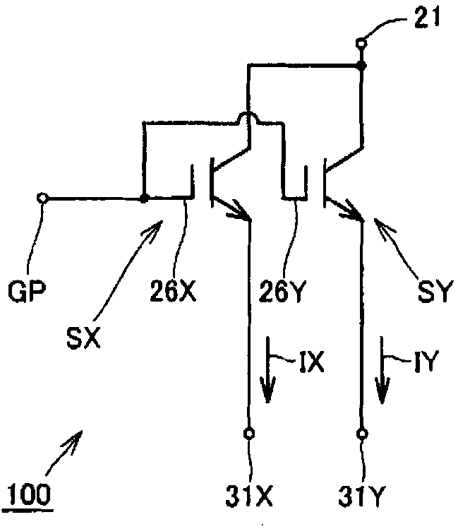
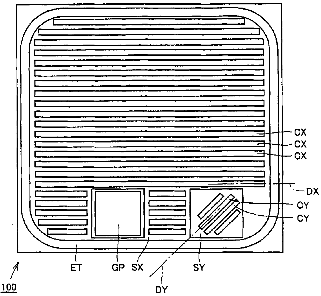
[0041] refer to figure 1 The semiconductor device 100 of the present embodiment is a power semiconductor device, and includes a main portion SX (first semiconductor element portion), a sense portion SY (second semiconductor element portion), and a gate pad GP. The main portion SX and the sense portion SY are IGBT portions that switch between the main current IX (first current) and the sense current IY (second current) in accordance with the voltage of the gate pad GP, respectively. The absolute value of the read current IY is smaller than the absolute value of the main current IX, for example, about 1 / 1000, and the waveform of the read current IY roughly corresponds to the waveform of the main current IX. Therefore, the sense current IY can be used as a current for monitoring whether the value of the main current IX is too large.
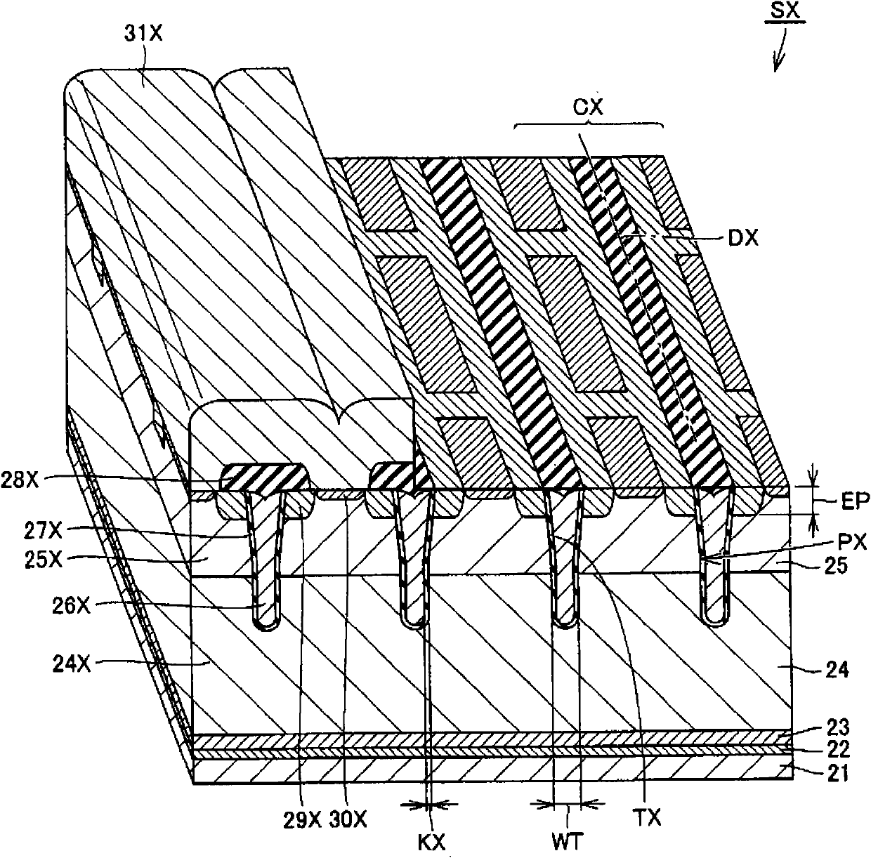
[0042] The main portion SX has a main gate electrode 26X serving as its gate electrode, a main emitter electrode 31X serving as its emitter electr...
Embodiment approach 2
[0085] main reference Figure 7 , in the semiconductor device of this embodiment instead of the readout section SY of Embodiment 1 ( Figure 4 ) has a readout unit SYa. The sensing section SYa has a connection with the sensing unit CY ( Figure 4 ) The readout unit CYa configured in the same way.
[0086] In addition, for each sense cell CYa, the sense part SYa replaces the sense part SY( Figure 4 ) readout n + Source portion 29Y which contains a sense n with + The reading n of the depth EPa different from the depth EP of the source portion 29Y + The source portion 29Ya. With this configuration, the main n of the main part SX of the semiconductor device of this embodiment + The depth EP of the source portion 29X (the first source portion) ( image 3 ) and the readout n of the readout section SYa + The depth EPa( Figure 7 ) are different from each other.
[0087] In addition, since the configuration other than the above is substantially the same as the configuratio...
Embodiment approach 3
[0100] In the semiconductor device of the present embodiment instead of the main part SX of the first embodiment ( image 3 ) and readout SY ( Figure 4 ) with the main part SXb ( Figure 11 ) and readout SYb ( Figure 12 ).
[0101] refer to Figure 11 , the main part SXb has a connection with the main unit CX ( image 3 ) similarly configured main unit CXb. In addition, for each main unit CXb, the main part SXb replaces the main part SX ( image 3 ) of the main n + source portion 29X and main p + Each part of the contact portion 30X has a main n + Source portion 29Xb and main p + Contact portion 30Xb. master n + Source portion 29Xb and main p + The contact portions 30Xb are arranged in stripes along the main direction DX in a planar view, and constitute a so-called stripe structure. master n + Source portion 29Xb and main p + The contact portions 30Xb each have a first source width WnX and a first contact width WpX along the main direction DX. Thus multiple m...
PUM
 Abstract
Description
Claims
Application Information
 - R&D Engineer
- R&D Manager
- IP Professional
- Industry Leading Data Capabilities
- Powerful AI technology
- Patent DNA Extraction
Browse by: Latest US Patents, China's latest patents, Technical Efficacy Thesaurus, Application Domain, Technology Topic, Popular Technical Reports.
© 2024 PatSnap. All rights reserved.Legal|Privacy policy|Modern Slavery Act Transparency Statement|Sitemap|About US| Contact US: help@patsnap.com