Method for reducing injury caused by laser peeling

A laser lift-off and laser scanning technology, applied in electrical components, semiconductor/solid-state device manufacturing, circuits, etc., can solve problems such as low yield, inability to fully realize the advantages of vertical structure LEDs, and performance degradation

Inactive Publication Date: 2010-12-22
INST OF SEMICONDUCTORS - CHINESE ACAD OF SCI
View PDF0 Cites 4 Cited by
  • Summary
  • Abstract
  • Description
  • Claims
  • Application Information

AI Technical Summary

Problems solved by technology

However, due to the mismatch between the lattice constant and the thermal expansion coefficient when the nitride is grown on the sapphire, the final nitride material on the sapphire has a high internal stress, which is manifested in the laser lift-off process, which is prone to cracks during the lift-off process, and the produced LED The leakage current of the chip is large, the performance decline cannot fully realize the advantages of the vertical structure LED, etc.
In the process of peeling off the self-supporting substrate, there are also problems such as fragility and low yield

Method used


Image

  • Method for reducing injury caused by laser peeling
  • Method for reducing injury caused by laser peeling
  • Method for reducing injury caused by laser peeling

Examples


Embodiment 1

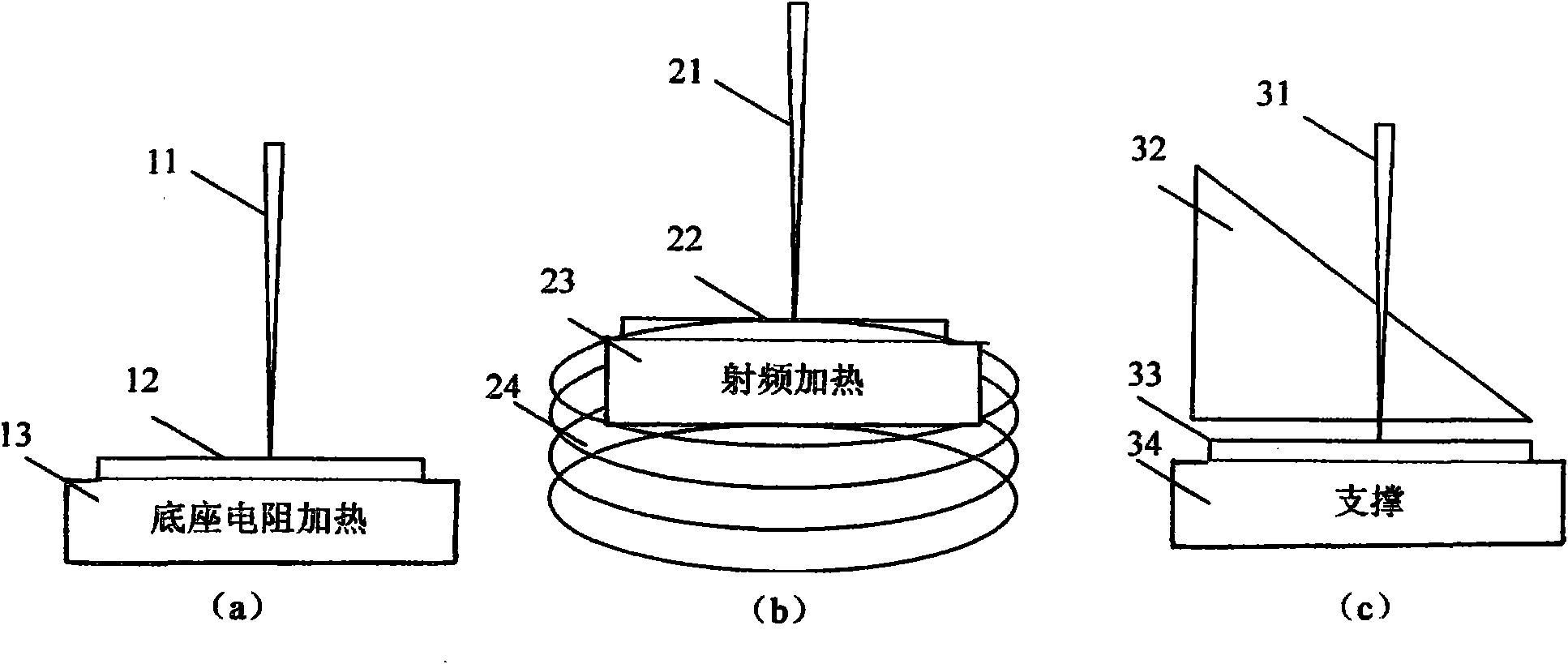
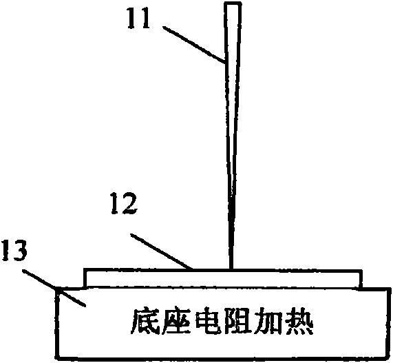
[0027] GaN / InGaN multiple quantum well LED structure on sapphire substrate, using such as figure 1 (a) shows the resistance heating of the bottom plate, 13 is the heated bottom plate, which is heated by resistance wire, and 12 is the GaN / InGaN multi-quantum well LED epitaxial wafer on the sapphire, which is placed on the heating plate 13, and reaches an appropriate temperature by heat conduction The temperature of the epitaxial wafer 12 can be obtained by thermocouple or non-contact infrared, laser temperature measurement, etc., and the stripping is carried out by scanning the laser 11 of the laser stripping equipment.

Embodiment 2

[0029] HVPE GaN thick film on sapphire substrate, using as figure 1 In the radio frequency heating shown in (b), 24 is a heated radio frequency coil, 23 is a heating base plate, which is heated by induction, and 22 is a GaN / InGaN LD epitaxial wafer on sapphire, which is placed on the heating base plate 23 and is induced by the heating base plate 23 After heating, the temperature of the epitaxial wafer 22 can be obtained through heat conduction to the epitaxial wafer 22. The temperature of the epitaxial wafer 22 can be obtained by thermocouple or non-contact infrared, laser temperature measurement, etc., and the self-supporting GaN substrate can be obtained by scanning with the laser 21 of the laser lift-off equipment. end.

Embodiment 3

[0031] GaN / AlGaN HEMT structures on sapphire substrates, using e.g. figure 1 The external light source shown in (c) is heated, 32 is the light source of external heating, 34 is the support base plate, 33 is the GaN / AlGaNHEMT epitaxial wafer on the sapphire, is placed on the support base plate 34, is heated by the external heating light source 32 epitaxial wafer 33 reaches For an appropriate temperature, the temperature of the epitaxial wafer 33 can be obtained by thermocouple or non-contact infrared, laser temperature measurement, etc., and the stripping is carried out by scanning the laser 31 of the laser stripping equipment.


PUM


Abstract

The invention provides a method for reducing the injury caused by laser peeling. The method comprises the following steps: step 1: loading an epitaxial wafer on a baseplate; step 2: heating the baseplate with the temperature of 100 to 600 DEG C in a manner of resistance heating, radio-frequency heating or external light source heating; and step 3: carrying out the laser peeling process on the epitaxial wafer by using the laser scanning of a laser peeling device, wherein the epitaxial wafer is particularly a photoelectron epitaxial material, a micro-electronic epitaxial material or a thick-film epitaxial material.

Description

technical field [0001] The invention belongs to the technical field of semiconductors, and is especially aimed at the laser lift-off technology of nitride optoelectronic materials, microelectronic materials or thick film materials. It controls the temperature of the epitaxial material so that the heterogeneous epitaxial material is in a stress-free or low-stress state. state, and then perform laser lift-off, which can minimize the lift-off damage of the epitaxial material. Background technique [0002] Group III nitride multi-system materials are semiconductor materials with direct band gaps. The band gap can be continuously adjusted from 0.7eV to 6.2eV, and the color covers from infrared to ultraviolet wavelengths. It can be used to prepare blue, green, and ultraviolet light-emitting diodes (LEDs), Optoelectronic devices such as short-wavelength laser diodes (LDs) have important applications in a wide range of fields such as high-density storage, display, and lighting. Esp...

Claims


Application Information

Patent Timeline
Patent Type & Authority Applications(China)
IPC IPC(8): H01L21/78H01L21/324H01L21/268H01L33/00
Inventor 段瑞飞王良臣刘志强季安王国宏曾一平李晋闽
Owner INST OF SEMICONDUCTORS - CHINESE ACAD OF SCI
Why Eureka
Try Eureka