Device and method for controlling temperature and uniformity of epitaxial wafers in MOCVD system
A technology of epitaxial wafer and uniformity, which is applied in gaseous chemical plating, metal material coating process, coating, etc., can solve the problems of mutual influence of temperature, unstable control of temperature and uniformity, and temperature uniformity of epitaxial wafer 400 Stability is difficult to guarantee and other problems, to achieve the effect of accurate measurement and guaranteed accuracy
- Summary
- Abstract
- Description
- Claims
- Application Information
AI Technical Summary
Problems solved by technology
Method used
Image
Examples
Embodiment 1
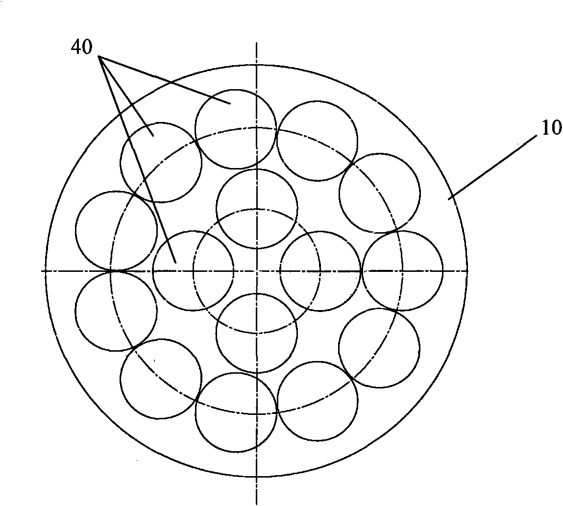
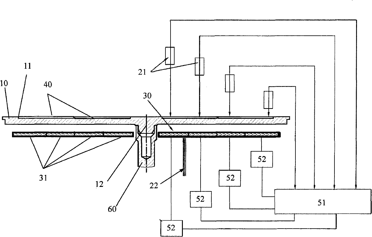
[0054] The device for controlling the temperature and uniformity of the epitaxial wafer 40 described in this embodiment is especially suitable for smaller-sized epitaxial wafers 40 with a diameter of 3 inches or less. Take 2 inches as an example, see image 3 , Figure 4 As shown, the device comprises a circular tray 10 ( image 3 ), correspondingly place 2-inch epitaxial wafers 40 in the plurality of concave discs 11, so that they are distributed and arranged in 4 annular regions with the same center but increasing radius on the upper surface of the tray 10 ( Figure 4 ), so that 54 epitaxial wafers 40 placed simultaneously on one tray 10 can be subjected to MOCVD coating treatment of multilayer epitaxial lattice structure thin films.
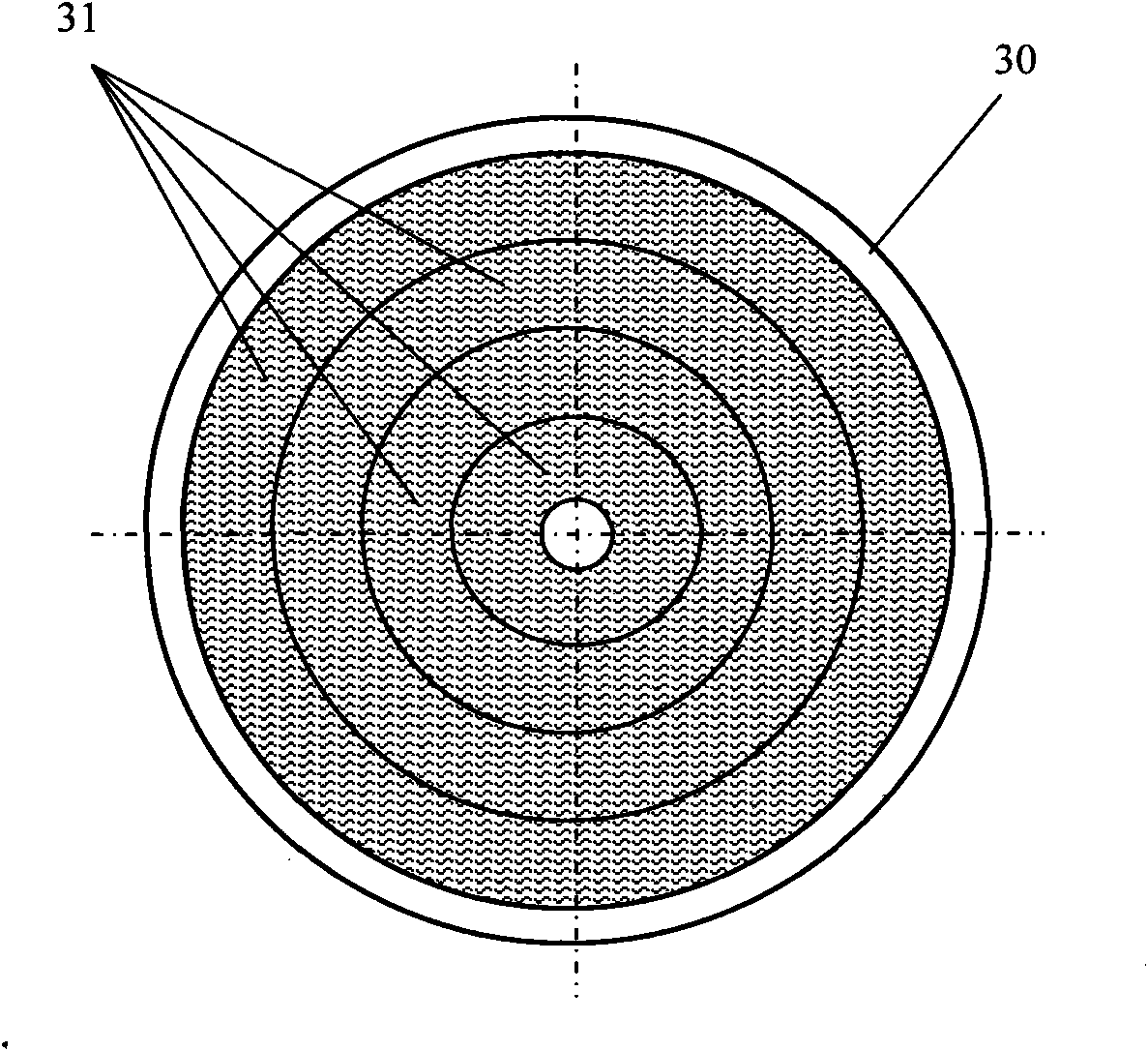
[0055] Cooperate see Figure 4 to Figure 6 As shown, a heater 30 is arranged below the tray 10, including 4 ring-shaped resistive heating elements 31 concentrically arranged ( Figure 5 ), each annular heating element 31 passes through the...
Embodiment 2
[0072] The device for controlling the temperature and uniformity of the epitaxial wafer 40 described in this embodiment is especially suitable for larger-sized epitaxial wafers 40 with a diameter of 4 inches or more. Cooperate see Figure 8 , Figure 9 As shown, similar to the above-mentioned embodiment, the device comprises a circular tray 10 ( Figure 8 ), a plurality of epitaxial wafers 40 with a diameter of 4 inches are correspondingly placed in the plurality of concave disks 11, so that they are distributed and arranged in two ring-shaped areas with the same center but increasing radii on the upper surface of the tray 10 ( Figure 9 ), so that 15 epitaxial wafers 40 placed simultaneously on one tray 10 can be subjected to MOCVD deposition treatment of multilayer epitaxial lattice structure thin films.
[0073] Cooperate see Figure 9 to Figure 11 As shown, a heater 30 is arranged under the tray 10 and is connected to at least one contact thermocouple thermometer 22 to ...
PUM
 Abstract
Description
Claims
Application Information
 - R&D
- Intellectual Property
- Life Sciences
- Materials
- Tech Scout
- Unparalleled Data Quality
- Higher Quality Content
- 60% Fewer Hallucinations
Browse by: Latest US Patents, China's latest patents, Technical Efficacy Thesaurus, Application Domain, Technology Topic, Popular Technical Reports.
© 2025 PatSnap. All rights reserved.Legal|Privacy policy|Modern Slavery Act Transparency Statement|Sitemap|About US| Contact US: help@patsnap.com


