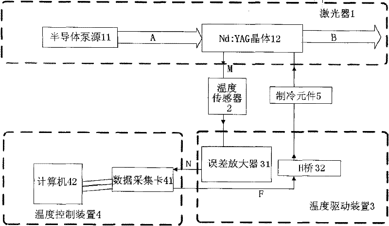
Semiconductor pumped full-cavity microchip laser device with stable output wavelength
A microchip laser and semiconductor technology, applied in the field of lasers, can solve problems such as laser temperature effects, and achieve the effects of accurate and stable laser wavelength, stable temperature, and high temperature control accuracy
- Summary
- Abstract
- Description
- Claims
- Application Information
AI Technical Summary
Problems solved by technology
Method used
Image
Examples
Embodiment 1
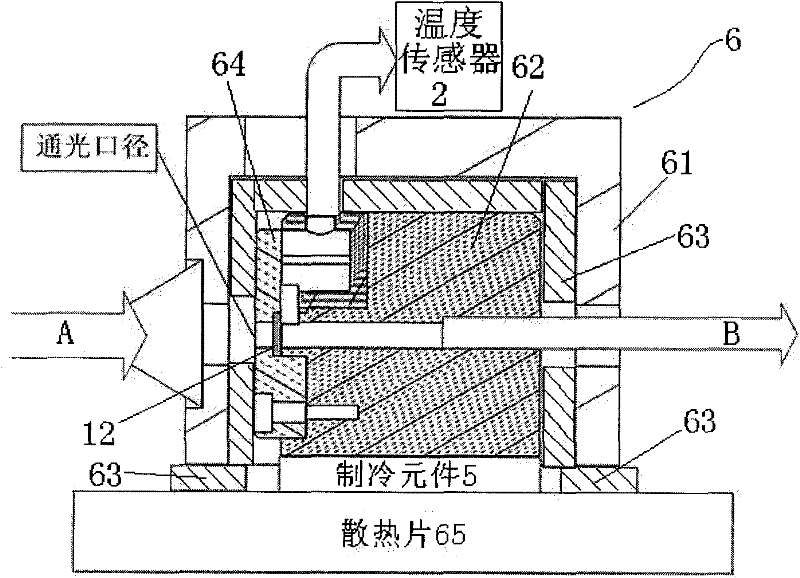
[0029] Embodiment 1: only Nd:YAG crystal 12 is provided with insulation space 6
[0030] Such as image 3 As shown, the thermal insulation space 6 of the present embodiment includes a base 62 arranged in a thermal insulation shell 61, a felt 63 for heat insulation is arranged between the base 62 and the thermal insulation shell 61, and the base 62 and the shell 61 A light hole is correspondingly arranged on the top, the pump beam A enters from one side, and the laser beam B outputs from the other side. The Nd:YAG crystal 12 is placed at the entrance of the light hole of the base 62 and fixed on the base 62 through a gland 64 . The temperature sensor 2 is also arranged in the heat preservation housing 61 , the temperature measuring probe of the temperature sensor 2 is attached to the Nd:YAG crystal 12 , and the electric lead of the temperature sensor 2 passes through the housing 61 . The cooling element 5 is disposed at the bottom of the base 62 , and a cooling fin 65 is disp...
Embodiment 2
[0031] Embodiment 2: heat preservation space 6,7 is set for semiconductor pump source 11 and Nd:YAG crystal 12 respectively
[0032] Such as Figure 5 As shown, in this embodiment, while the Nd:YAG crystal 12 is provided with the same heat preservation space 6 as the embodiment 1, a similar heat preservation space 7 can also be provided for the semiconductor pump source 11 . In the thermal insulation space 7, a temperature sensor 2' and a cooling element 5' identical to the temperature sensor 2 and the cooling element 5 are additionally set for the semiconductor pump source 11, and a temperature sensor 2 is set in the temperature driving device 3 to provide a driving current for the cooling element 5'. H-bridge 32'. The temperature sensor 2' on one side of semiconductor pump source 11 is connected in parallel with the temperature sensor 2 on one side of Nd:YAG crystal 12 to the same error amplifier 31; The cooling element 5 on one side of the YAG crystal 12 and the H-bridge ...
Embodiment 3
[0034] Embodiment 3: Semiconductor pump source 11 and Nd:YAG crystal 12 are arranged in the same heat preservation space 8
[0035] Such as figure 1 , Image 6 As shown, the thermal insulation space 8 of this embodiment includes a heat sink 81, a pump source base 82, a front plate 83, a crystal base 84, a crystal gland 85, a back plate 86, a window 87, an upper seat for adjustment 88 and a lower seat for adjustment 89. Both the front plate 83 and the back plate 86 are made of insulating material with a certain thickness and hardness, such as polytetrafluoroethylene, etc., and the heat sink 37 can be made of duralumin. The two sides of the window 87 are respectively coated with 1064nm anti-reflection coatings, so as to emit as much as possible the stable laser beam of the Nd:YAG crystal 12 with a wavelength of 1064nm. In this embodiment, the pump source base 82 , the Nd:YAG crystal base 84 and the crystal gland 85 can all be made of materials with good thermal conductivity, ...
PUM
 Abstract
Description
Claims
Application Information
 - R&D
- Intellectual Property
- Life Sciences
- Materials
- Tech Scout
- Unparalleled Data Quality
- Higher Quality Content
- 60% Fewer Hallucinations
Browse by: Latest US Patents, China's latest patents, Technical Efficacy Thesaurus, Application Domain, Technology Topic, Popular Technical Reports.
© 2025 PatSnap. All rights reserved.Legal|Privacy policy|Modern Slavery Act Transparency Statement|Sitemap|About US| Contact US: help@patsnap.com


