Packing alignment device for organic optoelectronic device and packing method thereof
A technology for optoelectronic devices and alignment devices, which is applied in the fields of electro-solid devices, photovoltaic power generation, electrical components, etc., can solve the problems of insufficient positioning accuracy of the substrate, and achieve easy control of the operation process, high precision, packaging method, and convenient operation. Effect
- Summary
- Abstract
- Description
- Claims
- Application Information
AI Technical Summary
Problems solved by technology
Method used
Image

Examples
Embodiment 1
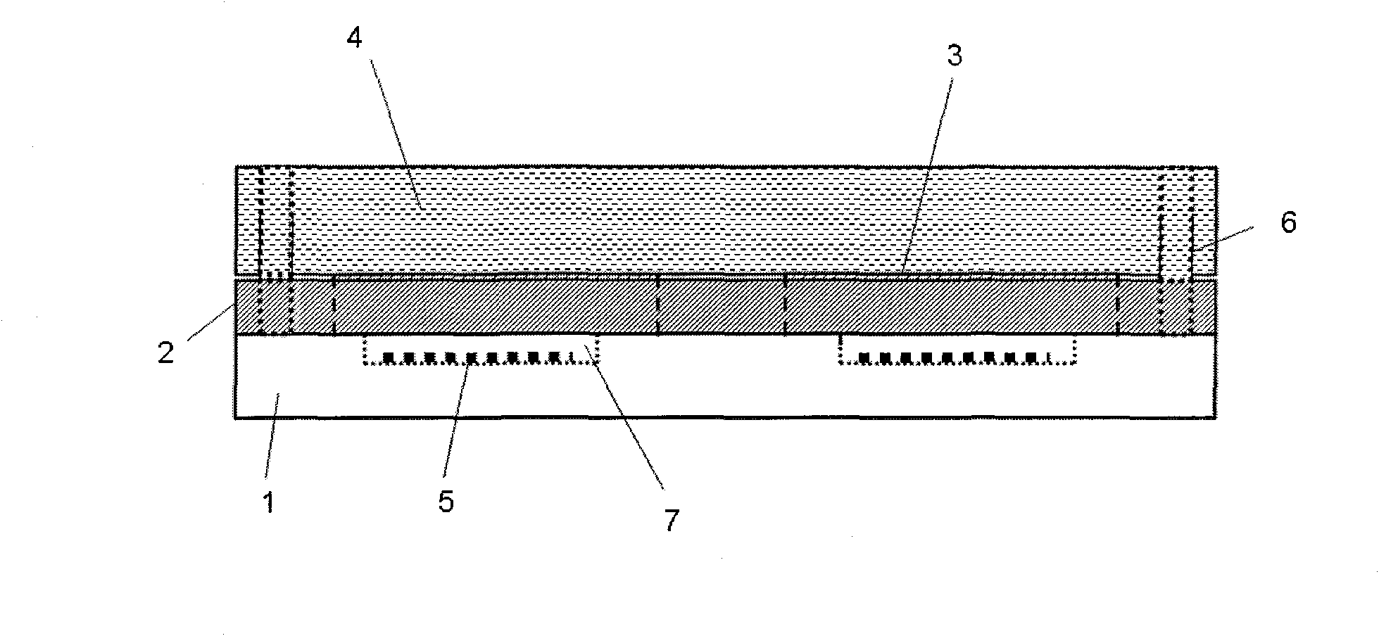
[0041] Such as Figure 4 The basic structure of the organic electroluminescent device (OLED) packaging system shown is that the device substrate is a glass substrate of 50mm×50mm, and the packaging cover plate is etched with soda-lime glass. The whole device structure is described as: glass substrate / ITO / NPB(50nm) / Alq3(30nm) / Mg:Ag(100nm).
[0042] The preparation method is as follows:
[0043] ①. Use acetone solution, deionized water and ethanol solution to ultrasonically clean the conductive substrate ITO glass, and dry it with dry nitrogen after cleaning. The ITO film on the glass substrate is used as the anode layer of the device, the square resistance of the ITO film is 12Ω / sq, and the film thickness is 180nm;
[0044] ②. Move the dried substrate into a vacuum chamber, and pretreat the ITO glass with low-energy oxygen plasma for 10 minutes under an oxygen pressure environment with an air pressure of 20Pa, and the sputtering power is 0-20W;
[0045] ③. Place the processe...
Embodiment 2
[0054] Such as Figure 4 The basic structure of the organic electroluminescent device (OLED) packaging system shown is that the device substrate is a glass substrate of 50mm×50mm, and the packaging cover plate is etched with soda-lime glass. The entire device structure is described as: glass substrate / ITO / CuPc(20nm) / α-NPD(60nm) / Alq 3 (40nm):C545T(2%) / Alq 3 (20nm) / Mg:Ag(100nm).
[0055] The preparation method is as follows:
[0056] ①. Use acetone solution, deionized water and ethanol solution to ultrasonically clean the conductive substrate ITO glass, and dry it with dry nitrogen after cleaning. The ITO film on the glass substrate is used as the anode layer of the device, the square resistance of the ITO film is 12Ω / sq, and the film thickness is 180nm;
[0057] ②. Move the dried substrate into a vacuum chamber, and pretreat the ITO glass with low-energy oxygen plasma for 10 minutes under an oxygen pressure environment with an air pressure of 20Pa, and the sputtering power ...
Embodiment 3
[0067] Such as Figure 4 The basic structure of the organic electroluminescent device (OLED) packaging system shown is that the device substrate is a glass substrate of 50mm×50mm, and the packaging cover plate is etched with soda-lime glass. The entire device structure is described as: glass substrate / ITO / PVK:PFC(100nm) / BCP(10nm) / Alq 3 (15nm) / Mg:Ag(100nm).
[0068] The preparation method is as follows:
[0069] ①. Use acetone solution, deionized water and ethanol solution to ultrasonically clean the conductive substrate ITO glass, and dry it with dry nitrogen after cleaning. The ITO film on the glass substrate is used as the anode layer of the device, the square resistance of the ITO film is 12Ω / sq, and the film thickness is 180nm;
[0070] ②. Move the dried substrate into a vacuum chamber, and pretreat the ITO glass with low-energy oxygen plasma for 10 minutes under an oxygen pressure environment with an air pressure of 20Pa, and the sputtering power is 0-20W;
[0071] ③....
PUM
 Abstract
Description
Claims
Application Information
 - R&D
- Intellectual Property
- Life Sciences
- Materials
- Tech Scout
- Unparalleled Data Quality
- Higher Quality Content
- 60% Fewer Hallucinations
Browse by: Latest US Patents, China's latest patents, Technical Efficacy Thesaurus, Application Domain, Technology Topic, Popular Technical Reports.
© 2025 PatSnap. All rights reserved.Legal|Privacy policy|Modern Slavery Act Transparency Statement|Sitemap|About US| Contact US: help@patsnap.com