
FFS (Fringe Field Switching) type TFT-LCD (Thin Film Transistor-Liquid Crystal Display) array substrate and manufacturing method thereof

An array substrate and substrate technology, applied in the field of liquid crystal displays, can solve the problems of light transmission, light leakage, FFS type array substrate can not ideally eliminate color drift and expand viewing angle, etc., so as to expand viewing angle, eliminate color drift and eliminate light leakage phenomenon Effect

Inactive Publication Date: 2010-09-29
BOE TECH GRP CO LTD +1
View PDF0 Cites 10 Cited by
  • Summary
  • Abstract
  • Description
  • Claims
  • Application Information

AI Technical Summary

Problems solved by technology

[0005] Theoretically, the increase in the number of domains is beneficial to expand the viewing angle and eliminate color drift, but Figure 21 The FFS-type array substrate shown cannot ideally eliminate color shift and further expand the viewing angle
Generally, for a normally black LCD, there is a small voltage difference between the pixel electrode and the common electrode when no power is applied. Figure 21 In the array substrate shown, since the pattern of the pixel electrode is a "herringbone" shape, the direction of the electric field formed between the pixel electrode and the common electrode is relatively consistent when the power is not applied, so the liquid crystal molecules will be more obviously deflected, resulting in light leakage. Generated, that is, when there is no electricity, the liquid crystal molecules are slightly deflected to cause light to pass through

Method used


Image

  • FFS (Fringe Field Switching) type TFT-LCD (Thin Film Transistor-Liquid Crystal Display) array substrate and manufacturing method thereof
  • FFS (Fringe Field Switching) type TFT-LCD (Thin Film Transistor-Liquid Crystal Display) array substrate and manufacturing method thereof
  • FFS (Fringe Field Switching) type TFT-LCD (Thin Film Transistor-Liquid Crystal Display) array substrate and manufacturing method thereof

Examples


Embodiment Construction

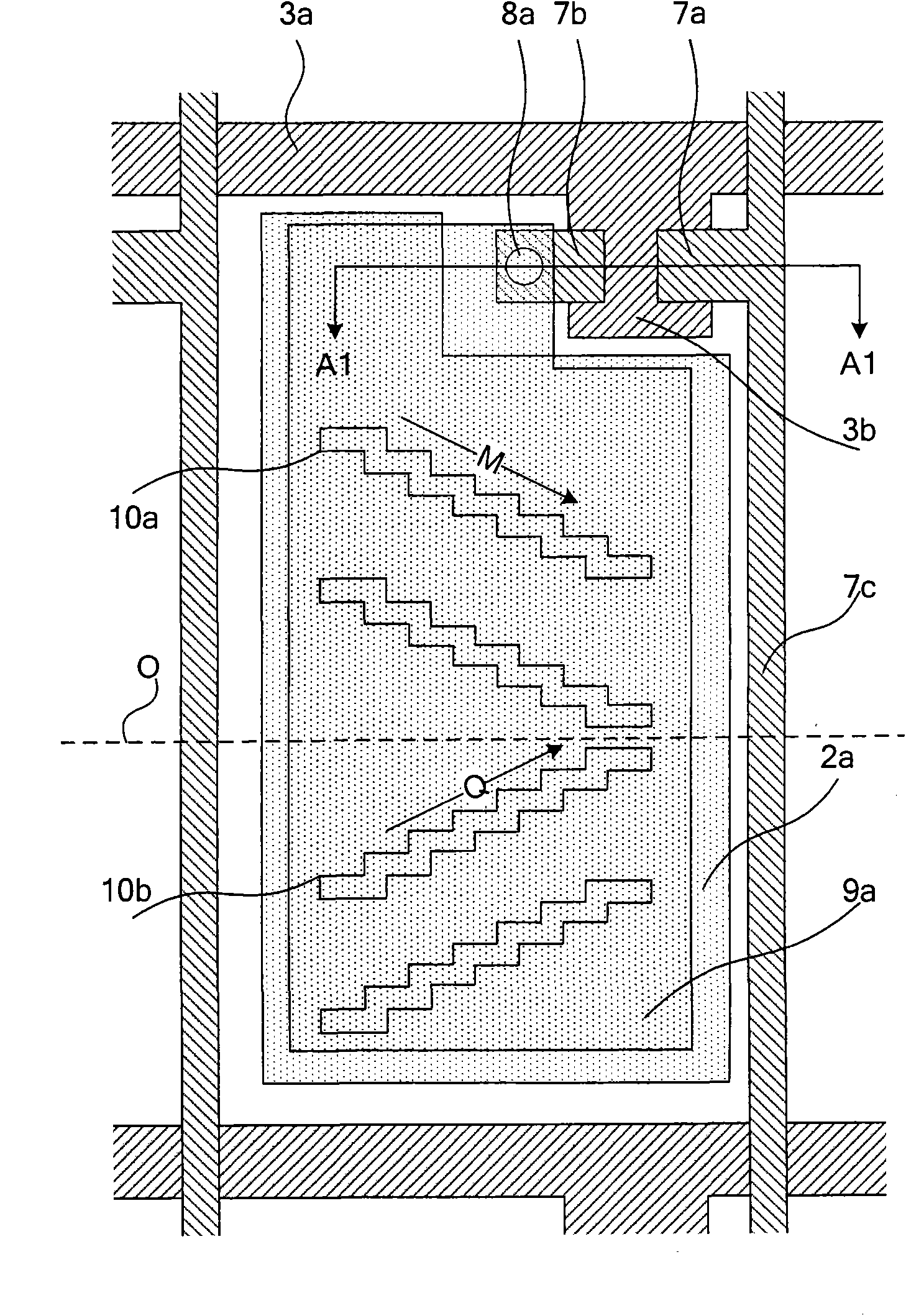
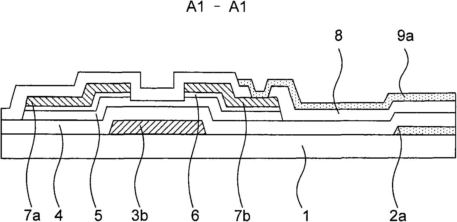
[0040] Figure 1a It is a plan view of the first embodiment of the FFS type TFT-LCD array substrate of the present invention, Figure 1b for Figure 1aMiddle A1-A1 section view. The structure of the FFS type TFT-LCD array substrate in this embodiment includes gate lines 3a and data lines 7c, and pixel electrodes 9a, common electrodes 2a and TFTs are formed in the pixel regions defined by the gate lines 3a and data lines 7c, and the TFTs include gate electrodes 3b , source electrode 7a, and drain electrode 7b, gate electrode 3b is formed on substrate 1, and is connected with gate line 3a; Gate insulating layer 4 is formed on gate electrode 3b and covers whole substrate 1; By semiconductor layer 5 and doped semiconductor layer The active layer composed of 6 is formed on the gate insulating layer 4 and located above the gate electrode 3b; the source electrode 7a is formed on the doped semiconductor layer 6, one end is located above the gate electrode 3b, and the other end is co...


PUM


Abstract

The invention discloses an FFS (Fringe Field Switching) type TFT-LCD (Thin Film Transistor-Liquid Crystal Display) array substrate and a manufacturing method thereof, comprising a grid line and a data line. A pixel electrode, a common electrode and a thin film transistor are formed in a pixel area limited by the grid line and the data line, wherein the pixel electrode and / or the common electrode are / is provided with a plurality of ladder-shaped strip-shaped grooves which enable a plurality of horizontal electric field in multiple directions to be formed between the pixel electrode and the common electrode, and each strip-shaped groove at least comprises two zigzag structures. In the FFS type TFT-LCD array substrate and the manufacturing method thereof, by setting the pixel electrode into figures comprising a plurality of ladder-shaped broken lines, a polydomain liquid crystal working mode can be provided, the visual angle is enlarged, and the color drifting can be eliminated.

Description

technical field [0001] The invention relates to liquid crystal display technology, in particular to a fringe field effect (Fringe Field Switching, FFS for short) type thin film transistor liquid crystal display (TFT-LCD) array substrate and a manufacturing method thereof. Background technique [0002] The FFS mode is a liquid crystal driving mode that can widen the viewing angle. The pixel electrodes in the FFS TFT-LCD array substrate are striped. When power is applied, a horizontal electric field parallel to the substrate is formed between the pixel electrodes and the common electrode. Such as Figure 19 Shown is a structural plan view of an FFS-type TFT-LCD array substrate in the prior art. Gate lines 22 and data lines 21 are formed on the array substrate. Adjacent gate lines 22 and data lines 21 define pixel areas, and each pixel The area is formed with a thin film transistor (TFT), strip-shaped pixel electrodes 24 and common electrodes 25. When no power is applied, there...

Claims


Application Information

Patent Timeline
Patent Type & Authority Applications(China)
IPC IPC(8): G02F1/1362G02F1/1343H01L27/12H01L21/84
CPCG02F1/133707G02F2001/134372H01L27/124G02F1/134372
Inventor 李文兵朴韩埈
Owner BOE TECH GRP CO LTD
Learn More