Experimental system for simulating single event effect (SEE) of pulse laser based on optical fiber probe

A technology of single event effect and fiber optic probe, which is applied in the direction of electronic circuit testing, components of electrical measuring instruments, measuring devices, etc., can solve the problem of large diameter of pulsed laser beam spot, and achieve the effect of reducing costs

Active Publication Date: 2010-09-15
NAT UNIV OF DEFENSE TECH
View PDF5 Cites 16 Cited by
  • Summary
  • Abstract
  • Description
  • Claims
  • Application Information

AI Technical Summary

Problems solved by technology

[0009] The technical problem to be solved by the present invention is to solve the problem that the pulse laser beam spot diameter is too large in the traditional pulse laser simulation single event effect experimental system...

Method used


Image

  • Experimental system for simulating single event effect (SEE) of pulse laser based on optical fiber probe
  • Experimental system for simulating single event effect (SEE) of pulse laser based on optical fiber probe
  • Experimental system for simulating single event effect (SEE) of pulse laser based on optical fiber probe

Examples


Embodiment Construction

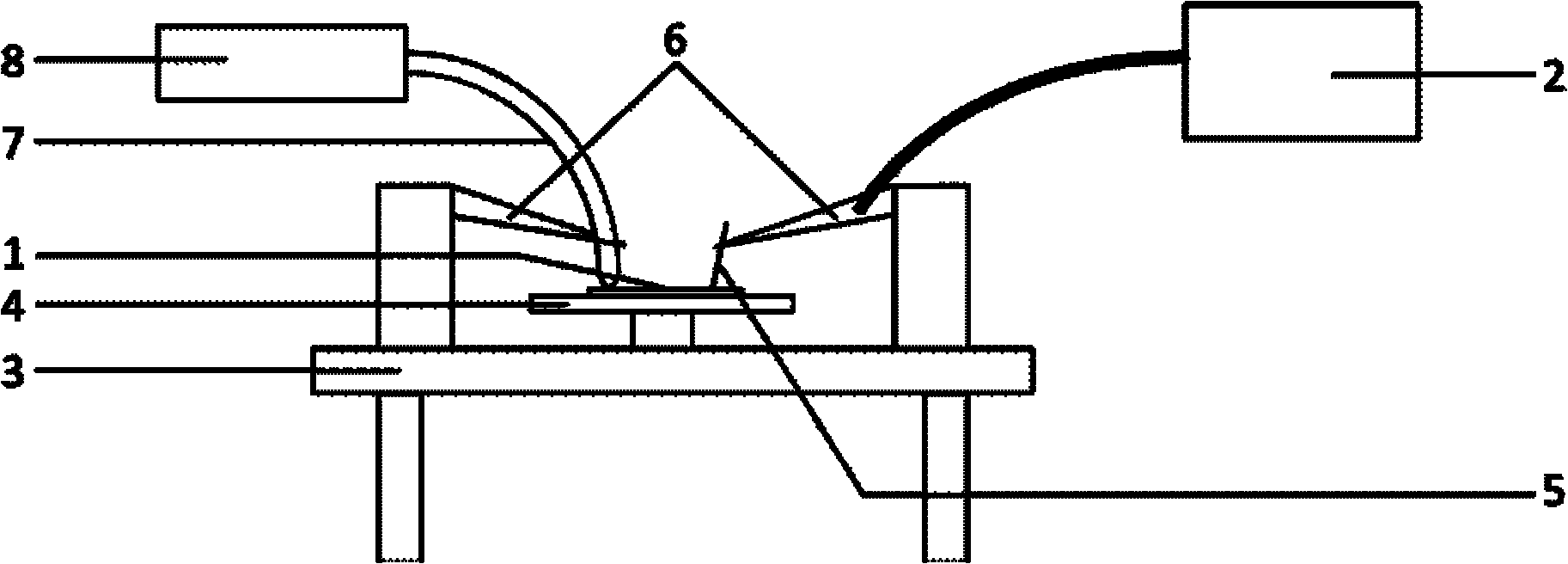
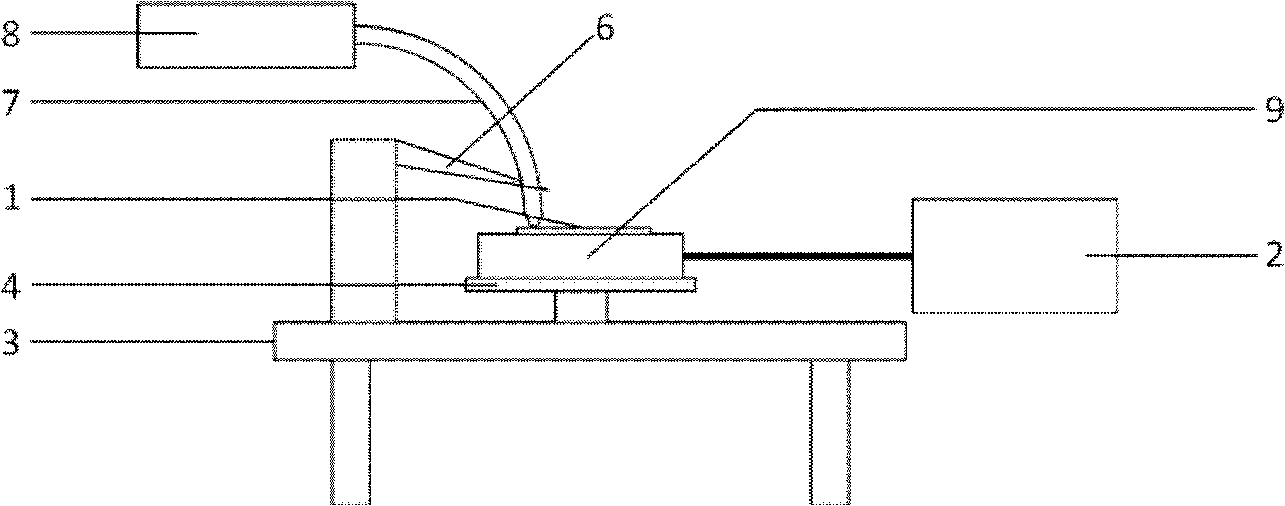
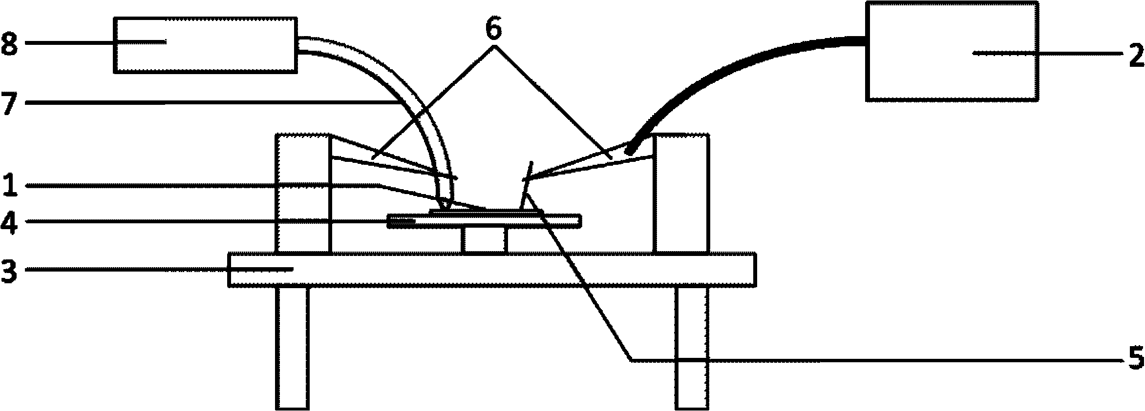
[0028] figure 1 It is a schematic diagram of the overall structure of the present invention when the tested integrated circuit chip 1 is not installed in the single event effect detection circuit board. The integrated circuit chip 1 to be tested is fixed on the sample support plate 4 of the probe station 3, and a plurality of electrical probes 5 of the probe station 3 are respectively fixed in a plurality of probe clips 6 of the probe station 3, and each electrical probe The tips of 5 respectively contact the input and output interfaces of the integrated circuit chip 1 under test, and the wires of each probe clip 6 are connected to the single event effect detection system 2 . The input end of the optical fiber probe 7 is connected to the pulsed laser 8, and a section of optical fiber near the output end of the optical fiber probe 7 is fixed in the probe holder 6 of the probe station 3, and the output end of the optical fiber probe 7 contacts the tested integrated circuit chip ...


PUM

PropertyMeasurementUnit
Wavelengthaaaaaaaaaa

Abstract

The invention discloses an experimental system for simulating a single event effect (SEE) of pulse laser based on an optical fiber probe, aiming to reduce beam spot diameter of the pulse laser and realize simulation of the SEE at a single device or a local circuit in a deep sub-micron integrated circuit. The system is composed of a pulse laser, an optical fiber probe and a probe platform, and the aperture of the conical tip of the optical fiber probe is 10nm-1mu m; the input end of the optical fiber probe is connected with the pulse laser, the optical fiber of the optical fiber probe close to the output end is fixed in a probe clip of the probe platform, the output end of the optical fiber probe is contacted with the detected position of an integrated circuit chip, and the optical fiber probe transmits the pulse laser to the output end from the input end; and the integrated circuit chip adopts two modes of being arranged or not arranged in a single event effect detection circuit board. By the invention, pulse laser with the beam spot diameter no more than 1 mu m can be output, thus realizing simulation of the SEE at a single device or a local circuit in a deep sub-micron integrated circuit and lowering the cost.

Description

technical field [0001] The invention relates to an experimental system for simulating single-particle effects with pulsed lasers, in particular to an experimental system for simulating single-particle effects with pulsed lasers based on fiber optic probes. Background technique [0002] The single event effect refers to the phenomenon that high-energy particles in space are incident on microelectronic devices or circuits in operation, causing logic errors, abnormal functions and even device damage. A large number of microelectronic devices and integrated circuits are used on the spacecraft. The safe and reliable operation of the spacecraft depends on the normal operation of these devices and circuits, and the orbiting spacecraft is always exposed to the impact of cosmic rays and high-energy particles in the earth's radiation belt. In radiation, once a single event effect occurs, it may cause fatal damage to the spacecraft. Therefore, it is of great significance to the develo...

Claims


Application Information

Patent Timeline
IPC IPC(8): G01R31/311G01R1/067
Inventor 池雅庆梁斌何益百刘必慰陈书明孙永节
Owner NAT UNIV OF DEFENSE TECH
Why Eureka
Try Eureka