High voltage low power consumption SOI LDMOS transistor having strained silicon structure

A low power consumption, transistor technology, applied in the direction of semiconductor devices, electrical components, circuits, etc., can solve the problems of limited interaction, super junction structure has not been widely used, and the impact of device breakdown voltage, etc., to meet the application requirements , Improving the mobility of electron carriers and reducing the drain-source on-resistance

Inactive Publication Date: 2011-11-16
HARBIN ENG UNIV
View PDF0 Cites 0 Cited by
  • Summary
  • Abstract
  • Description
  • Claims
  • Application Information

AI Technical Summary

Problems solved by technology

[0003] However, the charge of the p-type substrate contained in the LDMOS transistor participates in the charge compensation in the superjunction structure. Therefore, the breakdown voltage of the device is greatly affected, so that the superjunction structure has not been widely used in lateral power devices.
Salama et al. proposed to implant superjunction LDMOS (Patent No. US 6,768,180 B2) on the SOI structure, which effectively limits the interaction between the charge in the superjunction and the charge in the substrate

Method used


Image

  • High voltage low power consumption SOI LDMOS transistor having strained silicon structure
  • High voltage low power consumption SOI LDMOS transistor having strained silicon structure
  • High voltage low power consumption SOI LDMOS transistor having strained silicon structure

Examples


Embodiment Construction

[0019] The present invention is described in more detail below in conjunction with accompanying drawing example:

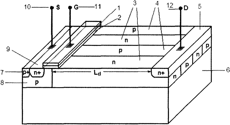
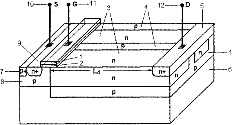
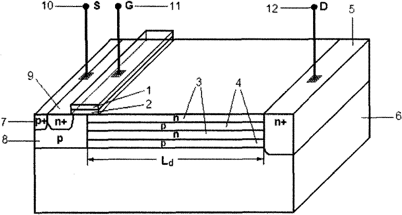
[0020] refer to figure 2 , SOI LDMOS transistor of the present invention. Including source region 9, body region 8, n-column 3 in superjunction, p-column 4 in superjunction, drain region 5, source electrode 10, drain electrode 12, gate electrode 11, buried dielectric layer 6 (SiO 2 or Al 2 o 3 and other insulating dielectric layers). It is characterized in that the p-column 4 is a single crystal material that does not match the silicon material lattice (such as Ge, SiGe and other materials that enable silicon to generate strain), and the n-column 3 is an n-type parallel to the p-column 4 generated on the basis of the p-column 4. Laterally tensile strained silicon for source and drain electrodes. In the super junction structure, the cross-section of the p-pillar 4 in the direction of the source and drain electrodes is a comb structure. According to the requi...


PUM


Abstract

The invention provides a high voltage low power consumption SOI LDMOS transistor having strained silicon structure, which comprises a source region (9), a body region (8), a drain region (5), a super-junction structure middle n column (3), a super-junction structure middle p column (4), a source electrode (10), a drain electrode (12), a grid electrode (11) and an embedded dielectric layer (6), wherein the super-junction structure middle p column (4) is silicon material lattice-unmatched monocrystal material, which is a material capable of leading silicon to generate strain, like Ge or SiGe, and the super-junction structure middle n column (3) is n-type transverse tensile strain silicon which is parallel to the source electrode and the drain electrode and generated on the basis of the super-junction structure middle p column (4). According to the invention, the requirement of reducing drain-source on-resistance is taken into consideration on the premise of maintaining the pressure resistance of devices. The transistor according to the invention is compatible with conventional SOI LDMOS transistor technology, has quite strong practicability and is easier for meeting the application requirement of power electronic system.

Description

technical field [0001] The invention relates to an electronic device, mainly a transistor. Specifically, it is a silicon-on-insulator (SOI) laterally diffused metal oxide semiconductor field effect transistor (LDMOSFET). Background technique [0002] In recent years, motor control, electronic ballasts, power supply switching modules and other related technologies have promoted the rapid development of smart power integrated circuits (SPICs). In SPIC, LDMOS devices play an important role. In the design of LDMOS devices, the primary considerations are breakdown voltage (BV) and on-resistance (R on ) compromise problem. Recently, a new type of device called Super Junction has attracted widespread attention due to its great improvement in the compromise between breakdown voltage and on-resistance compared to traditional devices. The concept of the superjunction is based on the complete charge compensation of alternate and heavily doped n and p columns in the drift region whe...

Claims


Application Information

Patent Timeline
Patent Type & Authority Patents(China)
IPC IPC(8): H01L29/78H01L29/06
Inventor 王颖胡海帆曹菲
Owner HARBIN ENG UNIV
Why Eureka
Try Eureka