Nonvolatile storage element, and method for manufacturing nonvolatile storage element or nonvolatile storage device

A technology of non-volatile storage and manufacturing method, applied in the field of non-volatile storage elements, can solve the problems of large size difference, non-uniformity of characteristics, and large non-uniformity of characteristics of non-volatile storage elements, etc. , to achieve the effect of shape shift and stability and small shape shift

Inactive Publication Date: 2010-08-04
PANASONIC CORP
View PDF2 Cites 0 Cited by
  • Summary
  • Abstract
  • Description
  • Claims
  • Application Information

AI Technical Summary

Problems solved by technology

[0006] Regarding the nonvolatile memory element of the conventional example, although there is no particular description of the electrode material used as the upper electrode or the lower electrode, there are certain restrictions on the electrode that reversibly changes the resistor, and it is limited to specific material
For example, in general, platinum (Pt), which is a representative etching-resistant material, is used for the upper electrode and the lower electrode, or for either one of the upper electrode and the lower electrode, to fabricate such a conventional electrode. In the case of a nonvolatile memory element such as the example, there is a tendency that although resistance change is likely to occur and the characteristics of the nonvolatile memory element are stabilized, since Pt is an etching-resistant material, if the conventional If the resist (resist) is used as a mask, the resist is etched during etching, and the size decreases, and the Pt becomes a tapered shape, and the size difference between the upper electrode and the lower electrode becomes larger, and the shape of the resistor changes. The bit becomes larger, so the non-uniformity of the characteristics of the nonvolatile memory element becomes larger
[0007] In addition, when a conductive material having an etching rate lower than that of a resist is used as a mask for etching Pt, the shape of etched Pt and the contact between the upper electrode and the lower electrode tend to be improved. Dimensional difference and displacement of the shape of the resistor, however, the mask becomes a tapered shape, and when the connector is connected to the upper electrode side in this state, the connection part becomes uneven because the connection part of the connector is not flat. Instability, which becomes the cause of non-uniformity of characteristics
[0008] Accordingly, the mask needs to be removed. However, since the mask is removed and the etching is performed, the interlayer film under the nonvolatile memory element is also etched, and it is difficult to control the excavation amount of the interlayer film. The shape of the permanent memory element becomes non-uniform, and the non-uniformity of characteristics becomes larger

Method used


Image

  • Nonvolatile storage element, and method for manufacturing nonvolatile storage element or nonvolatile storage device
  • Nonvolatile storage element, and method for manufacturing nonvolatile storage element or nonvolatile storage device
  • Nonvolatile storage element, and method for manufacturing nonvolatile storage element or nonvolatile storage device

Examples


Embodiment 1

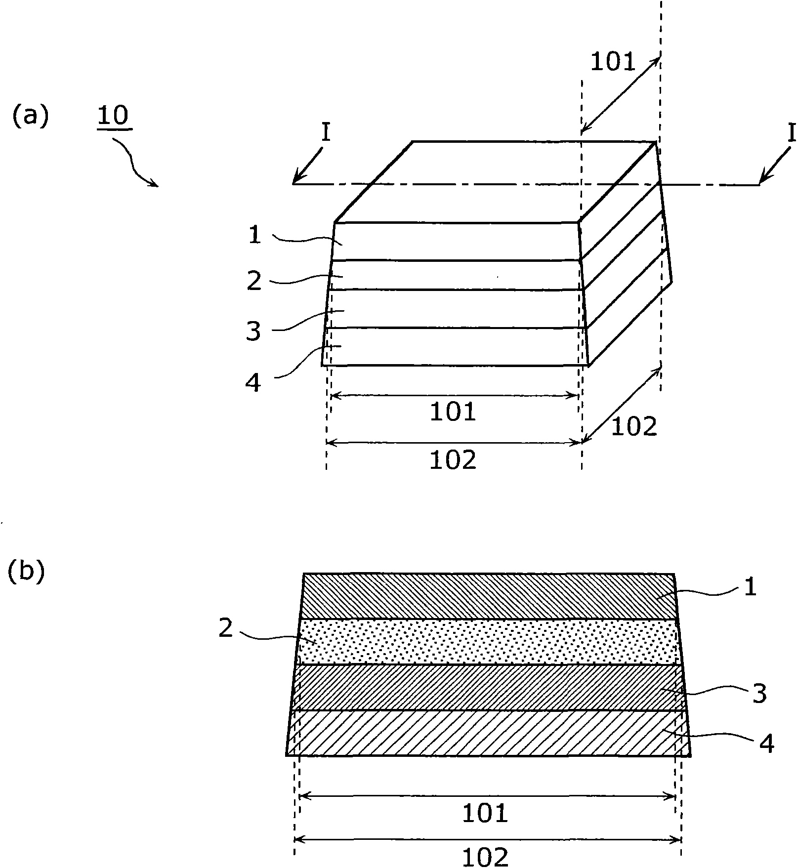
[0051] figure 1 (a) is a schematic perspective view showing the structure of the main part of the storage unit of the nonvolatile memory element 10 according to Embodiment 1 of the present invention, figure 1 (b) is shown along figure 1 (a) Cross-sectional view of the section along line I-I.

[0052] Such as figure 1 (a) and figure 1 (b) shows that the nonvolatile memory element 10 of the present invention includes the connection electrode layer 4 and the upper electrode layer 1 formed above the lower electrode layer 3 . The variable resistance layer 2 is formed between the upper electrode layer 1 and the lower electrode layer 3 .

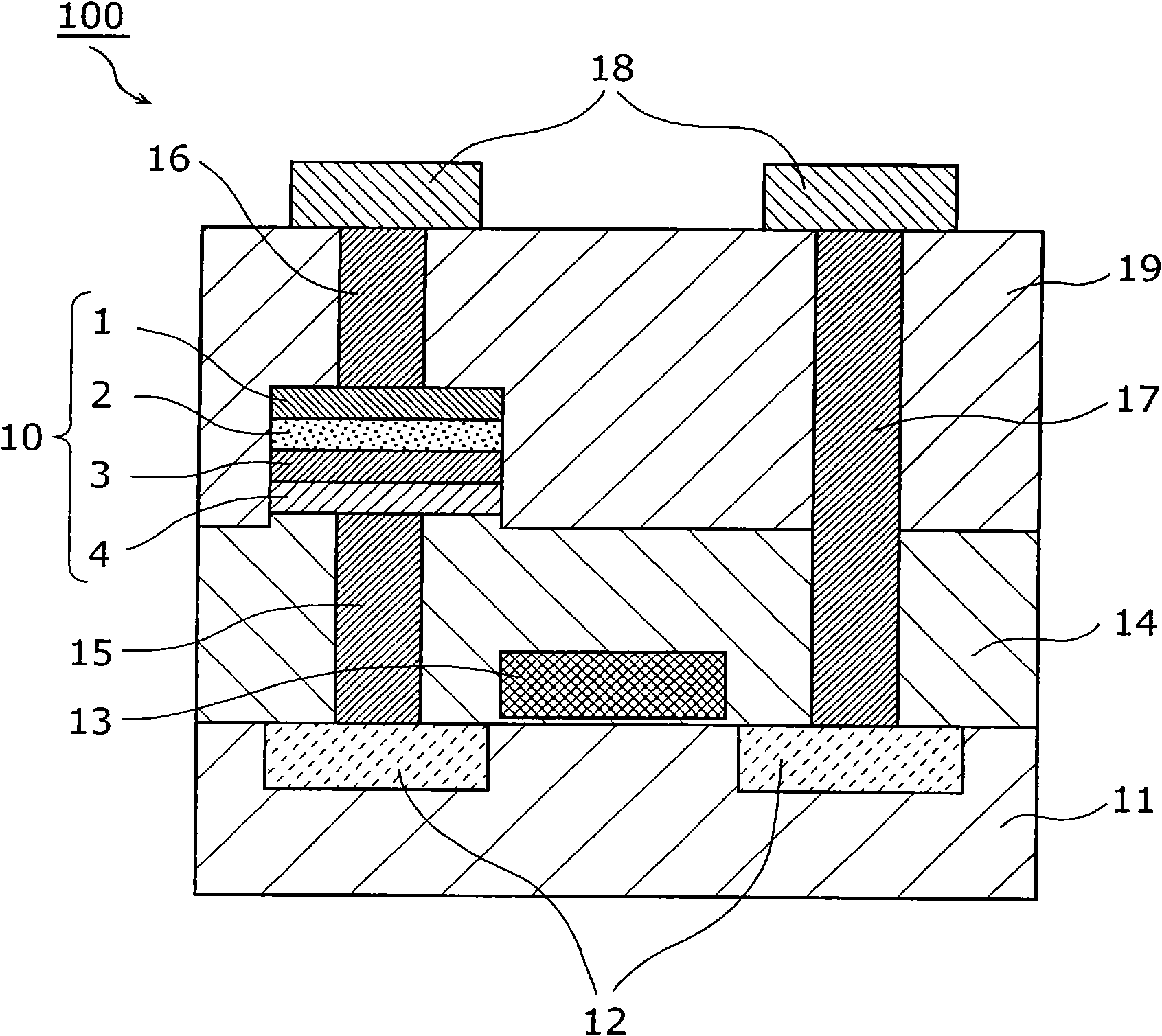
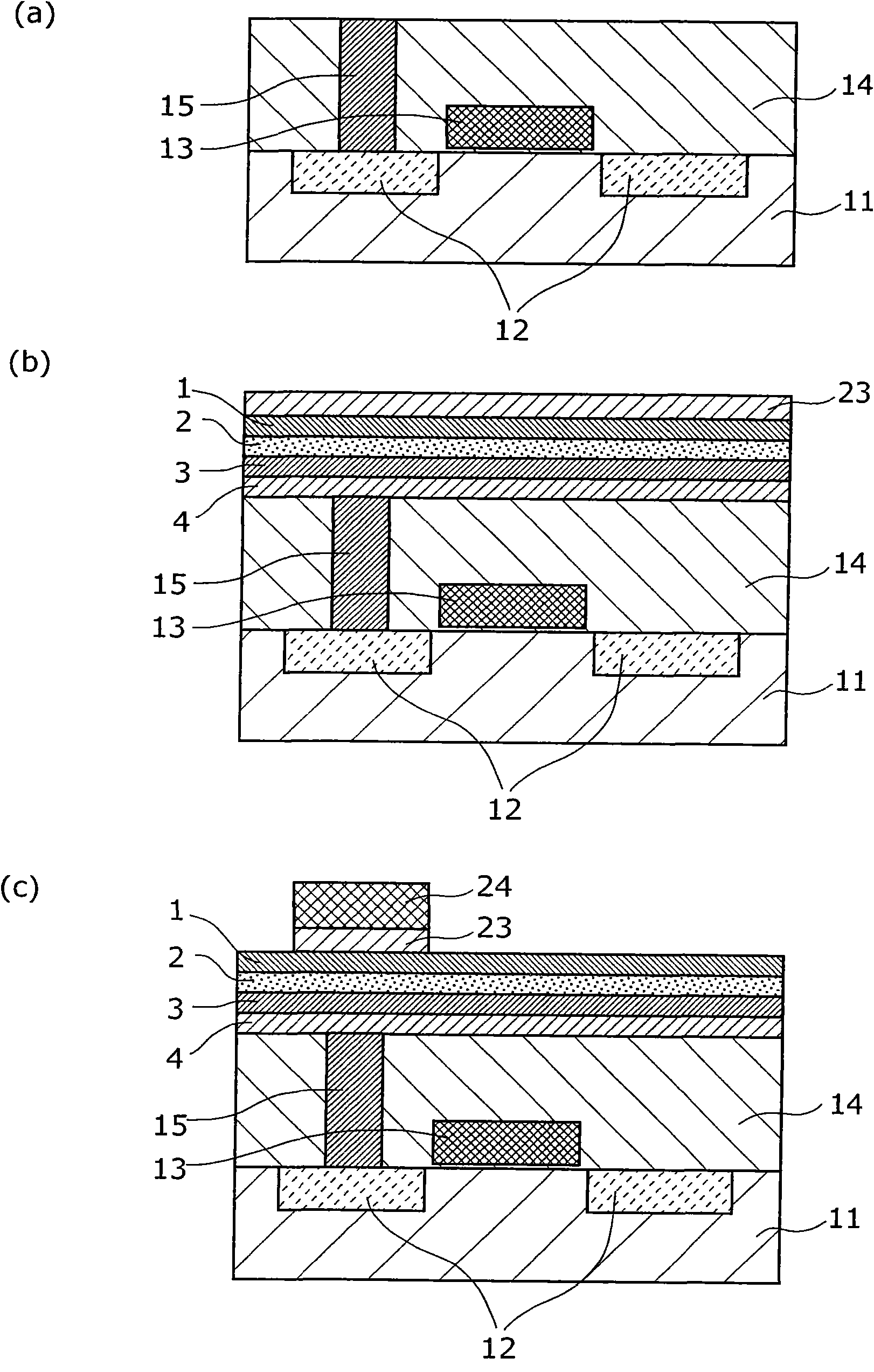
[0053] figure 2 It is a cross-sectional view showing a specific structure of a nonvolatile memory device 100 mounted with a nonvolatile memory element 10 according to Embodiment 1 of the present invention. Also, in general, many nonvolatile memory elements are formed over a substrate, but here, only one nonvolatile memory element is sho...

Embodiment 2

[0090] Figure 5 (a) is a schematic perspective view showing the structure of the main part of the storage unit of the nonvolatile memory element 20 according to Embodiment 2 of the present invention, Figure 5 (b) is shown along Figure 5 (a) Cross-sectional view of the II-II line cross section.

[0091] Such as Figure 5 (a) and Figure 5 (b) shows that the nonvolatile memory element 20 includes the upper electrode layer 1 formed above the connection electrode layer 4 . A variable resistance layer 2 is formed between these connection electrode layers and the upper electrode layer 1 .

[0092] and, Figure 6 It is also a cross-sectional view showing a specific structure of a nonvolatile memory device 200 mounted with a nonvolatile memory element 20 according to the second embodiment. Therefore, the upper electrode layer 1 formed above the connection electrode layer 4 is included. In the nonvolatile memory element 20 , the variable resistance layer 2 is formed between t...


PUM


Abstract

Provided is a method for manufacturing a nonvolatile storage element wherein a shape shift of an upper electrode and a lower electrode is reduced. The method has a step of depositing a a conductive connection electrode layer (4), a conductive lower electrode layer (3) composed of nonnoble metal oxide, a variable resistance layer (2), an upper electrode layer (1) composed of a noble metal and a mask layer (23), in this order; a step of forming the mask layer (23) in a prescribed shape; a step of forming the upper electrode layer (1), the variable resistance layer (2) and the lower electrode layer (3) in prescribed shapes by etching by using the mask layer (23) as a mask; and a step of removing the mask layer (23) and a region of the connection electrode layer (4) exposed by the etching at the same time.

Description

technical field [0001] The present invention relates to a nonvolatile memory element, a nonvolatile memory device, and a manufacturing method thereof that store data using a material whose resistance value changes reversibly when an electric pulse is applied. Background technique [0002] In recent years, with the development of digital technology of electronic equipment, in order to store data such as music, images, and information, the demand for larger-capacity and non-volatile storage elements has gradually increased. In order to meet these demands, attention has been paid to memory elements using a material whose resistance value is changed by an applied electric pulse and which can always maintain the state. [0003] Figure 9 It is a cross-sectional view of a main part showing the structure of an example of such a conventional nonvolatile memory element (for example, refer to Patent Document 1). Such as Figure 9 It is shown that the nonvolatile storage element is a ...

Claims


Application Information

Patent Timeline
Patent Type & Authority Applications(China)
IPC IPC(8): H01L27/10
CPCH01L45/04H01L45/1675H01L27/2436H01L45/146H01L45/145H01L45/1233H01L27/24H10B63/30H10N70/20H10N70/826H10N70/8833H10N70/063
Inventor 川岛良男三河巧高木刚有田浩二
Owner PANASONIC CORP
Why Eureka
Try Eureka