Ultra-thin light-emitting diode (LED) display

A technology of light-emitting diodes and displays, which is applied in the direction of instruments, electric solid-state devices, semiconductor devices, etc., and can solve problems such as high astigmatism rate and hazy light

Inactive Publication Date: 2010-06-23
陈宏铭
View PDF4 Cites 8 Cited by
  • Summary
  • Abstract
  • Description
  • Claims
  • Application Information

AI Technical Summary

Problems solved by technology

With such a structure, there are several points for improvement: 1. In order to obtain a current that emits light within a certain range, a resistor needs to be added in the structure to adjust the current; For the metal layer to input current to emit light, it is necessary to combine the bare LED die with the metal pad on the soft board by wire bonding; 3. When the bare LED die is fixed on the metal backing board, Put soft glue on it to protect its structure; 4. The second metal layer has a high astigmatism rate, which will make the light of the bare die of the light-emitting diode in the dot matrix layout state, and the light will be hazy.

Method used


Image

  • Ultra-thin light-emitting diode (LED) display
  • Ultra-thin light-emitting diode (LED) display
  • Ultra-thin light-emitting diode (LED) display

Examples


Embodiment Construction

[0031] In order to fully understand the technical content of the present invention, the technical solutions of the present invention will be further introduced and explained below in accordance with the drawings and in combination with the best embodiments of the present invention.

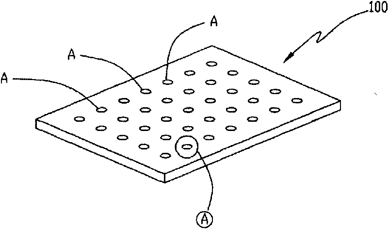
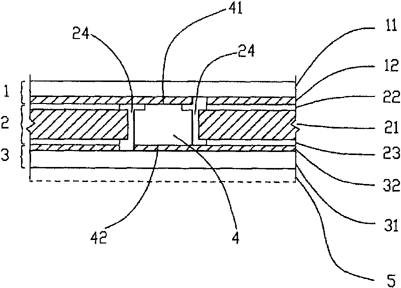
[0032] The ultra-thin light-emitting diode display 100 of the present invention is characterized in that it includes: a top layer 1, a middle layer 2, a bottom layer 3, and a plurality of light-emitting diode crystal grains 4; Layer 5.

[0033] Top layer 1, is a transparent film 11, and its base material is macromolecular transparent plastics, as polyethylene terephthalate (PET) or cyclic olefin copolymer (COC), on one side of transparent film 11, use vacuum evaporation Or sputter conductive substances, such as indium tin oxide (ITO), aluminum zinc oxide (AZO) or indium zinc oxide (IZO), as the transparent conductive film 12; Wet film and dry film wet film mixing method; using photoresist or phot...


PUM


Abstract

The invention relates to an ultra-thin light-emitting diode (LED) display. The display not only can be applied to single LED, but also can be applied to seven-segment displays, LED bars, dot matrix phalanxes and other special displays with specific patterns and design.

Description

technical field [0001] The present invention relates to an ultra-thin light-emitting diode display. The display of the present invention can be applied not only to a single light-emitting diode, but also to seven-segment displays, light-emitting diode display bars (Bar), dot matrix squares, and other specific Dedicated display for patterns and designs. Background technique [0002] This type of light-emitting diode display is currently known, such as the "flexible LED surface light source structure, flexible board, and manufacturing method thereof" announced by the patent bulletin I289947 (application 095109119) in Taiwan, such as figure 2 shown. The flexible LED surface light source structure includes: a flexible board with a first metal layer and a second metal layer, the first metal layer has a circuit layout, and the second metal layer is in a circular structure or fully Formed on the flexible board, and the second metal layer has a metal coating with high reflectivity...

Claims


Application Information

Patent Timeline
Patent Type & Authority Applications(China)
IPC IPC(8): G09F9/33H01L25/075H01L23/488
CPCH01L2224/48091H01L2224/48227H01L2924/00014
Inventor 张淇泽陈宏铭洪文仁
Owner 陈宏铭
Why Eureka
Try Eureka