
Alignment mark, making method and detection device thereof

A technique for aligning marks and manufacturing methods, which is applied in photolithographic process exposure devices, pattern surface photographic process, semiconductor/solid-state device manufacturing, etc., which can solve the problems of insufficient use of cutting lines and reduction of the use area of ​​front silicon wafers, etc. , to achieve accurate detection, reduce the front area of ​​the silicon wafer, and increase the utilization rate

Inactive Publication Date: 2010-03-31
SHANGHAI HUA HONG NEC ELECTRONICS
View PDF0 Cites 12 Cited by
  • Summary
  • Abstract
  • Description
  • Claims
  • Application Information

AI Technical Summary

Problems solved by technology

However, in the current process, the alignment marks are placed in the dicing lanes on the front side of the silicon wafer, which reduces the area used for the front side silicon wafer. Especially when developing a new process, there will be many layers on the front side of the silicon wafer. alignment marks, and the positions of the alignment marks are different
At this time, the cutting lanes for placing the alignment marks are often not enough

Method used


Image

  • Alignment mark, making method and detection device thereof
  • Alignment mark, making method and detection device thereof
  • Alignment mark, making method and detection device thereof

Examples


Embodiment Construction

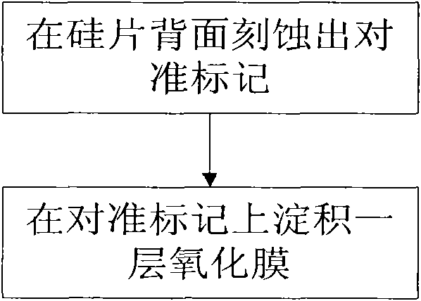
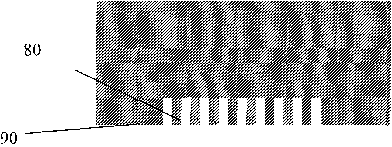
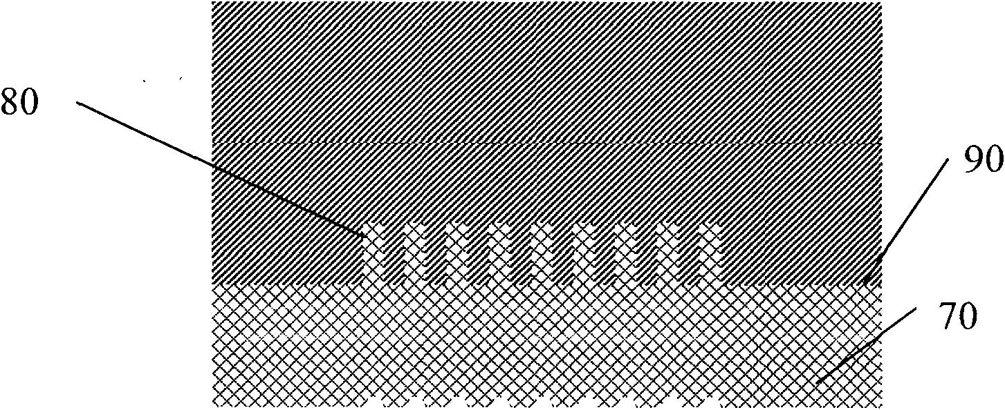
[0014] like Figure 1 to Figure 3 As shown, the manufacturing method of the alignment mark of the present invention includes two steps. First, photolithography is performed on the back surface 90 of the silicon wafer to etch a gate-shaped alignment mark. Secondly, a layer of oxide film 70 is deposited on the alignment mark. As a protective layer of the alignment mark, to prevent the alignment mark from being affected by other processes during the manufacturing process, the oxide film may be a silicon oxide film.

[0015] The alignment mark formed by the above method has a structure such as Figure 4 As shown, the alignment mark 80 is located on the back side 90 of the silicon wafer, and the alignment mark 80 is covered with an oxide film layer 70 that protects the alignment mark from being affected by other processes. The alignment mark of the present invention does not reduce the use of the front side of the silicon wafer. area.

[0016] like Figure 5 As shown, the detect...


PUM


Abstract

The present invention discloses a method for making alignment mark, comprising: 1) etching an alignment mark on the back side of a silicon chip; and 2) deposing a layer of oxide-film on the alignmentmark. The invention also discloses an alignment mark made by the method, which is arranged on the back side of a silicon chip. In addition, the invention further discloses a detection device for alignment mark, which comprises a light source, the light emitted by the light source passes through a half transparent and half reflecting mirror, is focused by a first convex lens, passes through a holeon a carrier corresponding to the alignment mark on the back side of a silicon chip, is focused to the alignment mark on the back side of the silicon chip, and is reflected by the alignment mark, signal light sent by the alignment mark passes through the half transparent and half reflecting mirror, and is focused by a second convex lens, and finally an imaged is formed on the plane of the detection device. An alignment mark made by the method is on the back side of a silicon chip, occupying no use area of the front side of the silicon chip, and the method for detecting an alignment mark can beused for detecting the alignment mark.

Description

technical field [0001] The invention relates to the technical field of semiconductor integrated circuit manufacturing, and in particular to an alignment mark, a method for making the alignment mark, and a detection device for the alignment mark. Background technique [0002] Alignment marks are often used in the field of semiconductor manufacturing. In the existing technology, the alignment marks are mainly placed in the dicing lines on the front side of the silicon wafer. Especially in the development of new processes, it is often necessary to add many alignment marks. batch to evaluate. However, in the current process, the alignment marks are placed in the dicing lanes on the front side of the silicon wafer, which reduces the area used for the front side silicon wafer. Especially when developing a new process, there will be many layers on the front side of the silicon wafer. alignment marks, and the positions of the alignment marks are different. At this time, the dicing...

Claims


Application Information

Patent Timeline
Patent Type & Authority Applications(China)
IPC IPC(8): G03F9/00G03F7/20H01L21/02
Inventor 陈福成
Owner SHANGHAI HUA HONG NEC ELECTRONICS
Learn More