
Electronic assemblies without solder and methods for their manufacture

A circuit assembly and component technology, which is applied in the direction of electrical components, electrical solid devices, and printed circuits assembled with electrical components, can solve problems such as high energy density that reduce the reliability of electronic products, and achieve improved mechanical shock resistance and improved design. , the effect of good performance

Inactive Publication Date: 2010-03-24
OCCAM PORTFOLIO LLC (US)
View PDF1 Cites 0 Cited by
  • Summary
  • Abstract
  • Description
  • Claims
  • Application Information

AI Technical Summary

Problems solved by technology

While such solutions offer benefits in certain applications, the chip's input / output (I / O) terminals can be very small and it becomes a challenge to precisely make such connections
Also, the finished device may not successfully pass the burn-in test, thus negating all previous efforts
[0019] Another area of ​​concern is thermal management, since densely packed ICs produce high energy densities that reduce the reliability of electronics

Method used


Image

  • Electronic assemblies without solder and methods for their manufacture
  • Electronic assemblies without solder and methods for their manufacture
  • Electronic assemblies without solder and methods for their manufacture

Examples


Embodiment Construction

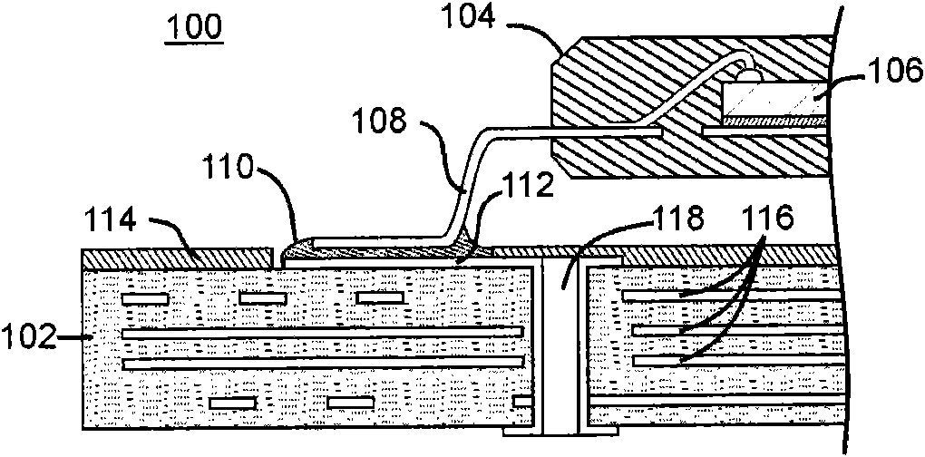
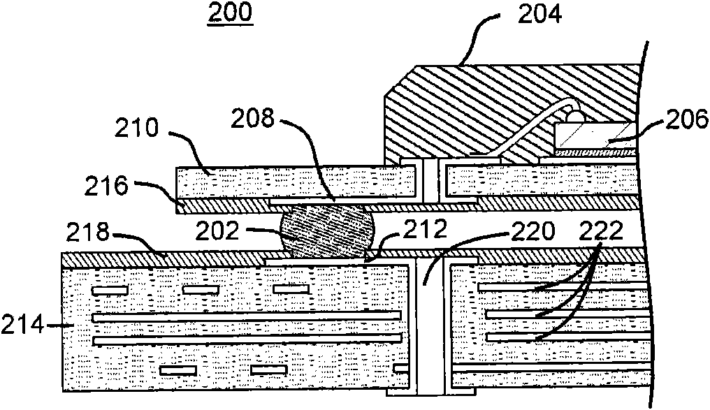
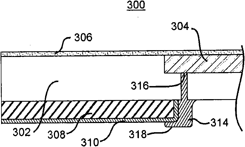
[0088] In the following description and accompanying drawings, specific terms and reference numerals are explained in detail to provide a thorough understanding of the present invention. In some instances, the terms and labels may contain specific details not required to practice the invention. For example, an interconnect between conductor elements of a component (i.e., an I / O lead of a component) may be shown or described as having multiple conductors interconnected to one lead or connected to multiple component contacts within or between devices. A conductor signal line. Thus, each of the plurality of conductor interconnections may alternatively be a signal, control, power or ground line of one conductor, and vice versa. Circuit paths shown or described as single-ended may also be different, and vice versa. Interconnect assemblies can consist of standard interconnects; microstrip or stripline interconnects and all signal lines of the assembly can be shielded or unshielded...


PUM


Abstract

Provided is an electronic assembly 400 and a method for its manufacture 800, 900, 1000 1200, 1400, 1500, 1700. The assembly 400 uses no solder. Components 406, or component packages 402, 802, 804, 806with I / O leads 412 are placed 800 onto a planar substrate 808. The assembly is encapsulated 900 with electrically insulating material 908 with vias 420, 1002 formed or drilled 1000 through the substrate 808 to the components' leads 412. Then the assembly is plated 1200 and the encapsulation and drilling process 1500 repeated to build up desired layers 422, 1502, 1702. The planar substrate 808 maybe a flexible substrate 2016 allowing bending of an assembly 2000 to fit into various enclosures.

Description

[0001] Cross References to Related Applications [0002] This application is a continuation of U.S. Application No. 12 / 163,870, filed June 27, 2008, which is a continuation of PCT Application No. PCT / US08 / 63123, filed May 8, 2008 Continuing the application in part and claiming its priority. PCT Application No. PCT / US08 / 63123 claims priority to: U.S. Application No. 60 / 928,467, "ELECTRONIC ASSEMBLY WITHOUT SOLDER," filed May 8, 2007; U.S. Application No. 60 / 928,467, filed May 29, 2007 60 / 932,200 "ELECTRONIC ASSEMBLY WITHOUT SOLDER AND METHODS FOR THEIR MANUFACTURE"; U.S. Application No. 60 / 958,385 "SOLDERLESS FLEXIBLEELECTRONIC ASSEMBLIES AND METHODS FOR THEIR MANUFACTURE" filed July 5, 2007; .60 / 959,148“ELECTRONIC ASSEMBLIES WITHOUT SOLDER AND METHODS FORTHEIR MANUFACTURE”;2007年7月31日提交美国申请No.60 / 962,626“MASS ASSEMBLY OF ENCAPULSATED ELECTRONIC COMPONENTSTO A PRINTED CIRCUIT BOARD BY MEANS OF AN ADHESIVE LAYERHAVING EMBEDDED CONDUCTIVE JOINING MATERIALS "; U.S. Application No.60...

Claims


Application Information

Patent Timeline
IPC IPC(8): H05K1/18
CPCH01L2924/01029H01L2924/01079H01L2924/01013H01L2924/15311H01L2924/19105H01L2224/32225H01L2224/32245H01L2224/48227H01L2224/48247H01L2224/48465H01L2224/73265H01L2924/00H01L2924/00012H01L23/48H05K3/32
Inventor 约瑟夫·C·菲耶尔斯塔德
Owner OCCAM PORTFOLIO LLC (US)
Learn More