
Electroluminescent device having improved power distribution

A technology of electroluminescence device and light-emitting layer, which is applied in the direction of electroluminescence light source, electric light source, lighting device, etc., can solve the problems of reducing the clarity of the device, and achieve the effect of improving contrast and improving power distribution

Inactive Publication Date: 2010-03-24
EASTMAN KODAK CO
View PDF11 Cites 14 Cited by
  • Summary
  • Abstract
  • Description
  • Claims
  • Application Information

AI Technical Summary

Problems solved by technology

The efficiency of the LED device is improved, but the trapped light may travel a considerable distance horizontally through the covering, substrate or layer in the EL unit before being scattered out of the device, reducing the Sharpness of the device in pixellated applications (eg displays)

Method used


Image

  • Electroluminescent device having improved power distribution
  • Electroluminescent device having improved power distribution
  • Electroluminescent device having improved power distribution

Examples


Embodiment Construction

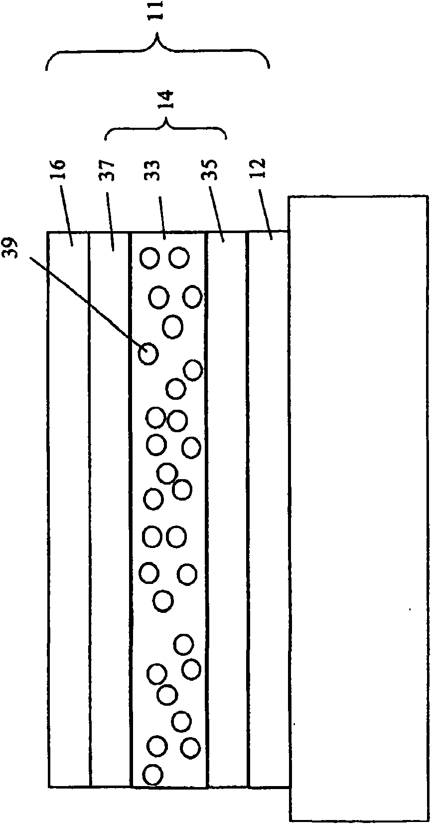
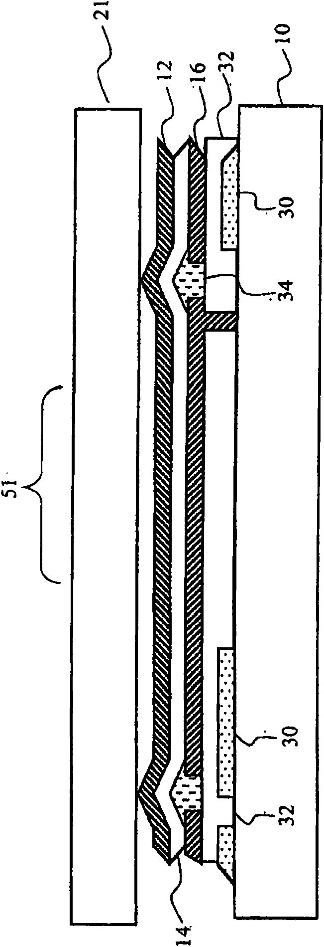
[0057] refer to figure 1 , in one top emitting embodiment of the present invention, the electroluminescent device comprises first and second electrodes 12 and 16 having an EL cell 14 formed therebetween, in said At least one layer in the EL cell is a light emitting layer comprising quantum dots, and the coextensive conductive regions of said first and second electrodes 12 and 16 define one or more light emitting regions. In the illustrated embodiment, the electrode 16 comprises a reflective element 20 and a transparent portion 22 in said light emitting area. The transparent portion 22 of the second electrode 16 is generally a relatively low conductive portion and through which the light 50a emitted by the light-emitting organic layer passes; the reflective portion 20 is generally a relatively high conductive portion and The emitted light 50b is reflected. The second electrode 16 can also be said to have two sides, adjacent the first side 6 and the second side 8 of the EL uni...


PUM


Abstract

The invention relates to an electroluminescent device comprising a first electrode and a second electrode having an EL unit formed there-between, wherein the EL unit comprises a light-emitting layer containing quantum dots, and the first and second electrodes define one or more light-emitting areas; wherein at least a portion of the second electrode is transparent and light emitted by the EL unitis viewed from a first side of the electroluminescent device that is nearer the second electrode; and one or more reflective elements that are electrically-conductive and are formed as part of the second electrode or in electrical communication with the second electrode; and wherein the reflective elements are located at least partially within the light emitting areas.

Description

technical field [0001] The present invention relates to electroluminescent devices, and more particularly to electroluminescent device structures for improved light output, contrast and power distribution. Background technique [0002] Semiconductor light emitting diode (LED) devices, which are primarily inorganic, have been manufactured since the early 1960's and are now manufactured for a variety of consumer and commercial applications. The layers containing the LEDs are based on crystalline semiconductor materials. These crystal-based inorganic LEDs have the advantages of high brightness, long lifetime, and excellent environmental stability. The crystalline semiconductor layers that offer these advantages also have a number of disadvantages. The most important disadvantages are the high manufacturing cost, the difficulty in combining multi-color outputs from the same chip, the efficiency of light output, and the need for costly rigid substrates. [0003] In the mid-198...

Claims


Application Information

Patent Timeline
Patent Type & Authority Applications(China)
IPC IPC(8): H01L51/52H05B33/22
CPCH05B33/22H01L51/5271B82Y20/00B82Y30/00H01L2251/5369H10K2102/331H10K59/878H10K50/856
Inventor R·S·科克
Owner EASTMAN KODAK CO
Learn More