Active area structure

A technology of active area and interconnection structure, applied in the direction of electrical components, electric solid-state devices, circuits, etc., can solve the problem of large leakage current between the source selection gate and the second type of active area, and achieve the compact structure of NAND devices and the area Small, solve the effect of power consumption increase

Active Publication Date: 2010-02-24
SEMICON MFG INT (SHANGHAI) CORP
View PDF0 Cites 2 Cited by
  • Summary
  • Abstract
  • Description
  • Claims
  • Application Information

AI Technical Summary

Problems solved by technology

[0007] The technical problem to be solved by the present invention is to provide an active region structure, which can solve the problem of large leakage current between the source selection gate and the second type of active region due to the damage of the gate oxide layer under the source selection gate interconnection structure

Method used


Image

  • Active area structure
  • Active area structure
  • Active area structure

Examples


Embodiment Construction

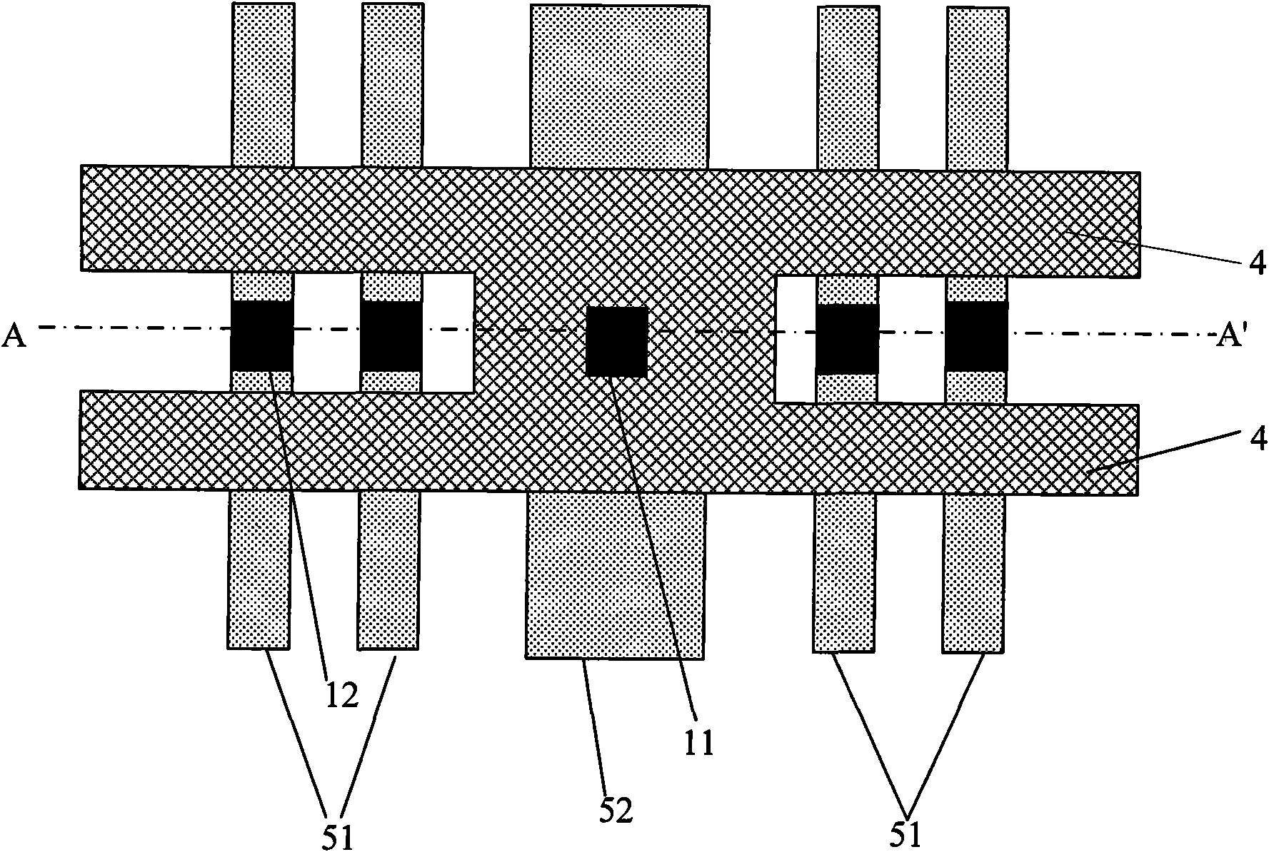
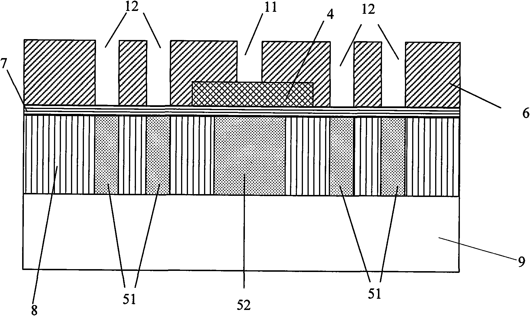
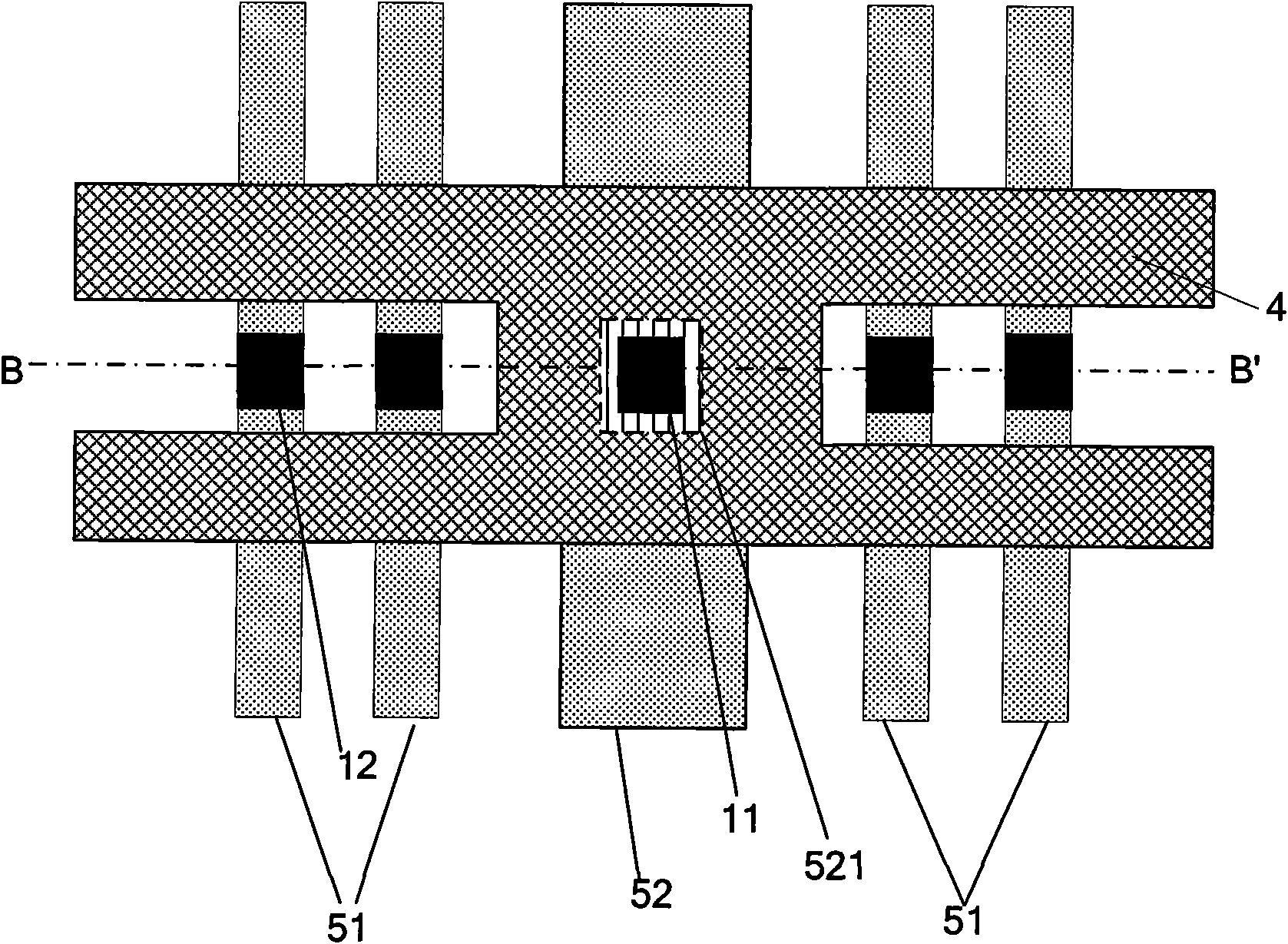
[0016] image 3 It is a partial layout diagram of the NAND device source selection gate in the embodiment of the present invention. From image 3 The layout shown shows active regions within the semiconductor substrate. The active area includes a first type active area and a second type active area. As in the background art, in this embodiment, the first type of active region is the memory cell active region 51 , and the second type of active region is the well lead-out active region 52 as an example. The active selection gate 4 is formed on the memory cell active area 51 and the well extraction active area 52 . An interconnection structure—active region contact hole 12 is formed on the active region 51 of the memory cell. An interconnection structure—source selection gate contact hole 11 is formed on the source selection gate 4 . The active area under the source selection gate contact hole 11 is the well extraction active area 52 . As described in the background, when t...


PUM


Abstract

The invention relates to an active area structure. An active area is a second type active area in a semiconductor substrate; the surface of the second type active area is covered with a gate oxide layer; the gate oxide layer is provided with a source selecting gate corresponding to the position of the second type active area; the second type active area also comprises an insulator well area; and the insulator well area corresponds to the position of an interconnecting structure for connecting the source selecting gate. By arranging the insulator well area at the position of the interconnectingstructure corresponding to the source selecting gate in the second type active area, the active area structure can effectively increase resistance between the source selecting gate and the second type active area under the source selecting gate and improve the insulated isolation performance between the both, thereby solving the problem of big leakage current between the source selecting gate andthe active area caused by the damage of the gate oxide layer under the interconnecting structure of the source selecting gate, reducing the power consumption of a NAND device, and improving the stability of the device.

Description

technical field [0001] The invention relates to the manufacturing field of NAND logic (hereinafter referred to as NAND) flash memory devices, in particular to the structure of the active region under the source selection gate contact hole of NAND. Background technique [0002] The NAND flash memory device is a common storage device in the current consumer electronics market, and it is a voltage-controlled device. Based on the tunnel effect, the device realizes data writing and erasing by charging and discharging its own floating gate. [0003] see figure 1 The shown NAND involves a layout diagram of a source selection gate (Source Selection Gate: SSG) part. Such as figure 1 The layout shown schematically illustrates active regions fabricated within a semiconductor substrate. The active area is divided into the first type of active area: the active area used to manufacture memory cell devices; the second type of active area: the active area of ​​the non-memory cell device...

Claims


Application Information

Patent Timeline
Patent Type & Authority Applications(China)
IPC IPC(8): H01L27/115
Inventor 蔡建祥
Owner SEMICON MFG INT (SHANGHAI) CORP
Why Eureka
Try Eureka