


Quick Research
Generate reliable direction feasibility study reports for your R&D in just a few steps.

Technical Q&A
Discover and master advanced knowledge NOW. Basics, ideas, possibilities, all at once.

Find Solutions
As an expert in R&D theories, this can generate solutions to your technical problems instantly.

Evaluate Feasibility
Analyze your overall solution with one click, know your potential R&D risks in advance.

Monitor Landscape
Get weekly tech updates, stay abreast of the latest tech innovations and key insights.
PCB, mould and LED display device
A PCB board and mold technology, which is applied in the field of LED lighting devices, can solve the problems of compatible display screen display effects, long proofing cycle, and long time required, etc.
- Summary
- Abstract
- Description
- Claims
- Application Information
AI Technical Summary
Problems solved by technology
Method used
Image


Examples
Embodiment 1
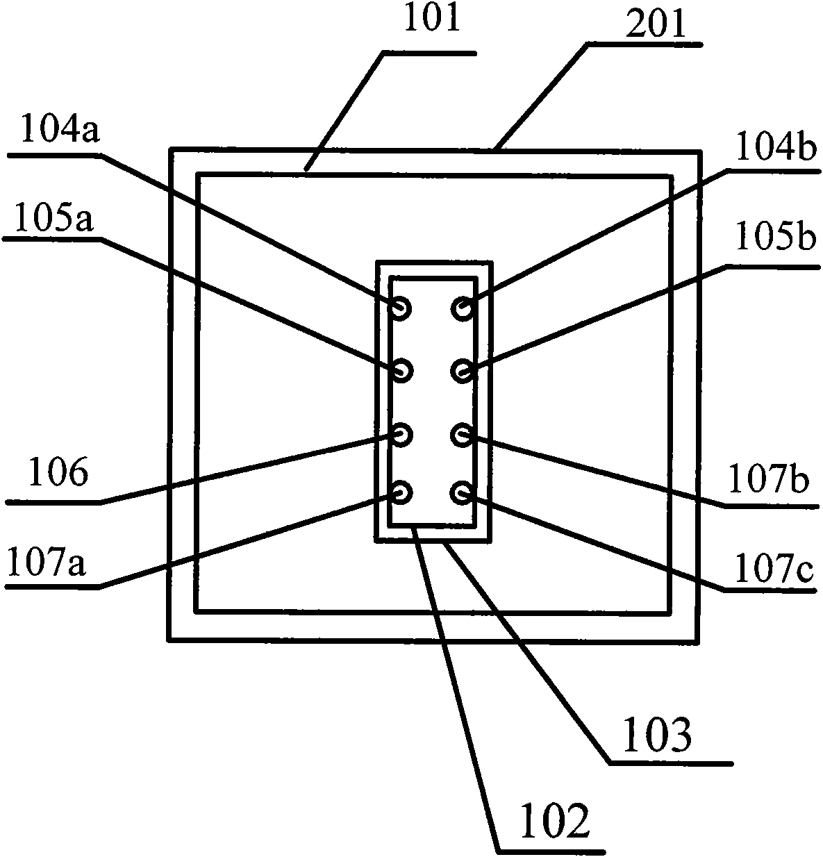
[0023] Such as figure 1 As shown, this embodiment provides a PCB board 101, and the PCB board 101 is provided with at least a power line interface, a signal line interface and at least one installation position.
[0024] On the PCB board, other electronic components can also be set according to actual needs, for example, several resistor combinations are set to prevent a certain component from burning out due to excessive current, or capacitors are set; the power line interface is connected to the PCB The power line provided on the board is electrically connected, and the power line is used to provide a voltage source for the electronic components on the PCB; and, a ground wire can also be provided to guide the excess current or strong potential generated by the PCB board into the ground, In addition, multiple ground wires can be set according to actual needs, so as to prevent excessive current or strong electric potential from causing harm to the human body.
[0025] At leas...
Embodiment 2
[0036] On the basis of the above examples, in the PCB board described in this embodiment, the first mounting position is also provided with at least two subordinate mounting positions for fixedly fitting and connecting at least two first integrated circuit control chips, for example, using The two first integrated circuit control chips are fixedly connected, that is, each slave installation position corresponds to a first integrated circuit control chip, and is used for installing the corresponding first integrated circuit control chip.
[0037] The two subordinate installation positions can be arranged in parallel in a row or in a row, and can also be set to be partially overlapped, and each line pin interface is respectively arranged on the two subordinate installation positions for electrical connection with the two first integrated circuit control chips and signal connection.
[0038] For example, the first integrated circuit control chip is a general integrated circuit co...
Embodiment 3
[0042] On the basis of the above examples, the dual-adaptation pin interface is set as two rows of parallel pin interfaces, and the first integrated circuit control chip and the second integrated circuit control chip are both provided with main signal lines. The control module is used to control each LED light-emitting diode according to the LED control signal transmitted by the main signal line. The input pin interface of the main signal line is set at the first row of pin interfaces, and the input of the main signal line is used to transmit the main signal; the output pin of the main signal line is set at the second row of pin interfaces.
[0043] The second integrated circuit control chip is also provided with a control module of a slave signal line, connected to at least one slave signal, the input pin interface of the slave signal line is set at the second row of pin interfaces, and the output pin interface of the slave signal line It may be arranged on the pin interface ...
PUM
 Abstract
Description
Claims
Application Information
 - R&D Engineer
- R&D Manager
- IP Professional
- Industry Leading Data Capabilities
- Powerful AI technology
- Patent DNA Extraction
Browse by: Latest US Patents, China's latest patents, Technical Efficacy Thesaurus, Application Domain, Technology Topic, Popular Technical Reports.
© 2024 PatSnap. All rights reserved.Legal|Privacy policy|Modern Slavery Act Transparency Statement|Sitemap|About US| Contact US: help@patsnap.com