
Process wall for glue spreading development equipment

A technology of gluing and development and process wall, which is applied to the photoplate making process of pattern surface, optical mechanical equipment, photography, etc., can solve the problems of limited transmission angle, slow transmission speed, inconvenient transmission, etc., and achieve the improvement of effective utilization rate, The effect of reducing work stations and occupying a small area

Active Publication Date: 2009-12-30
SHENYANG KINGSEMI CO LTD
View PDF1 Cites 8 Cited by
  • Summary
  • Abstract
  • Description
  • Claims
  • Application Information

AI Technical Summary

Problems solved by technology

This structure enables the cassette station robot and the process robot to transfer the wafer in one direction, and the transfer angle is limited, which brings inconvenience to the transfer; and the transfer speed is slow and the efficiency is low

Method used


Image

  • Process wall for glue spreading development equipment
  • Process wall for glue spreading development equipment
  • Process wall for glue spreading development equipment

Examples


Embodiment

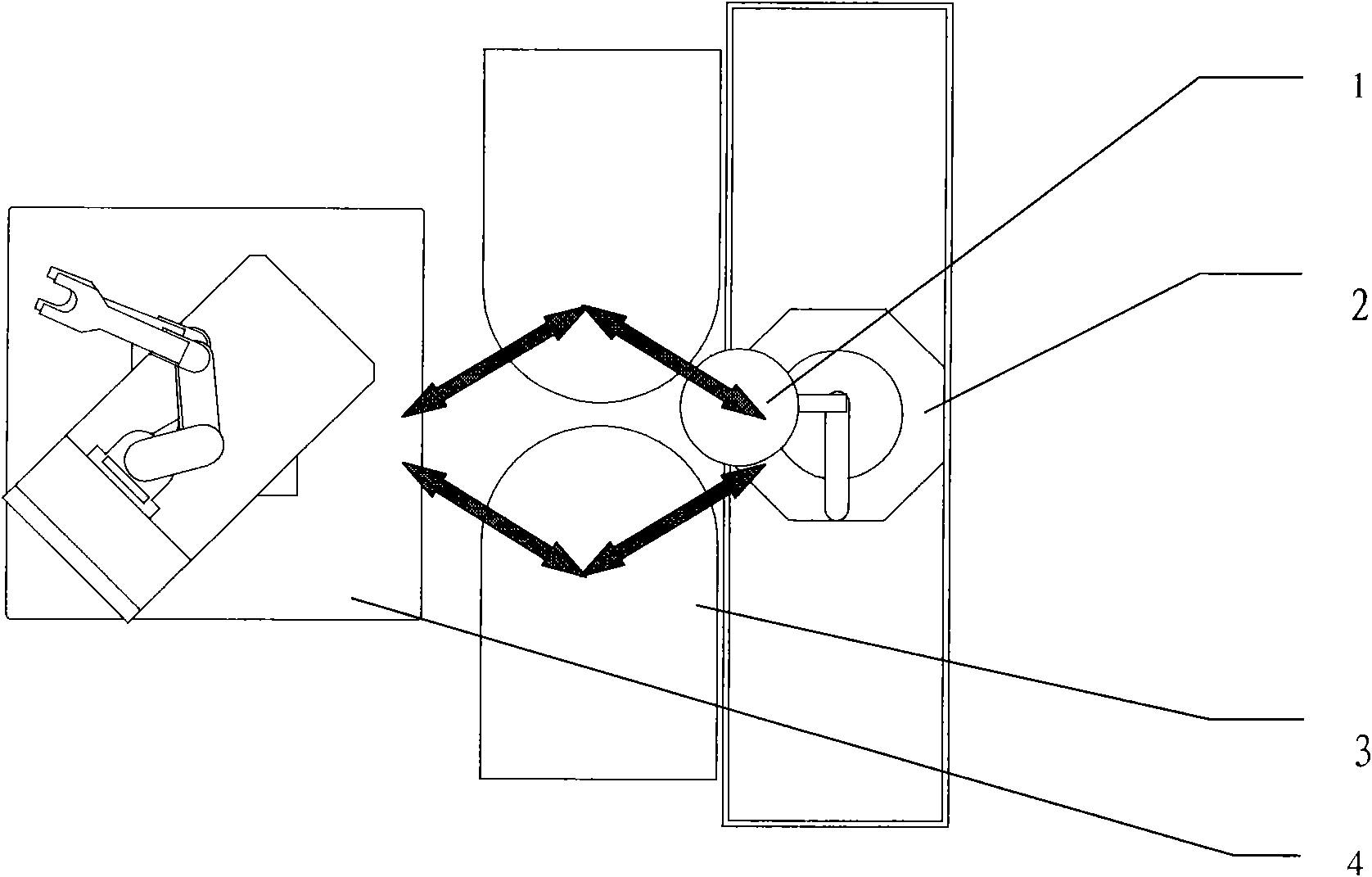
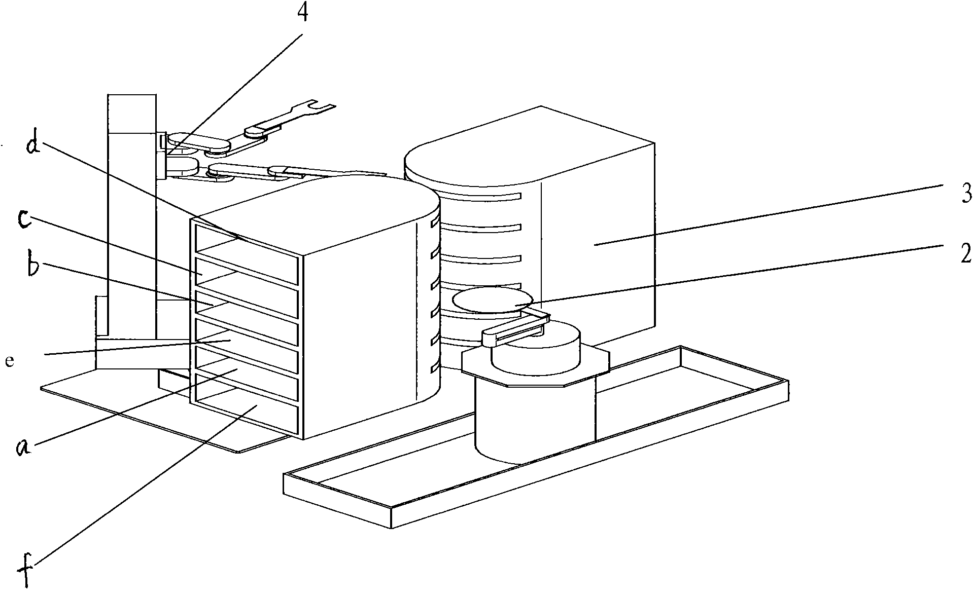
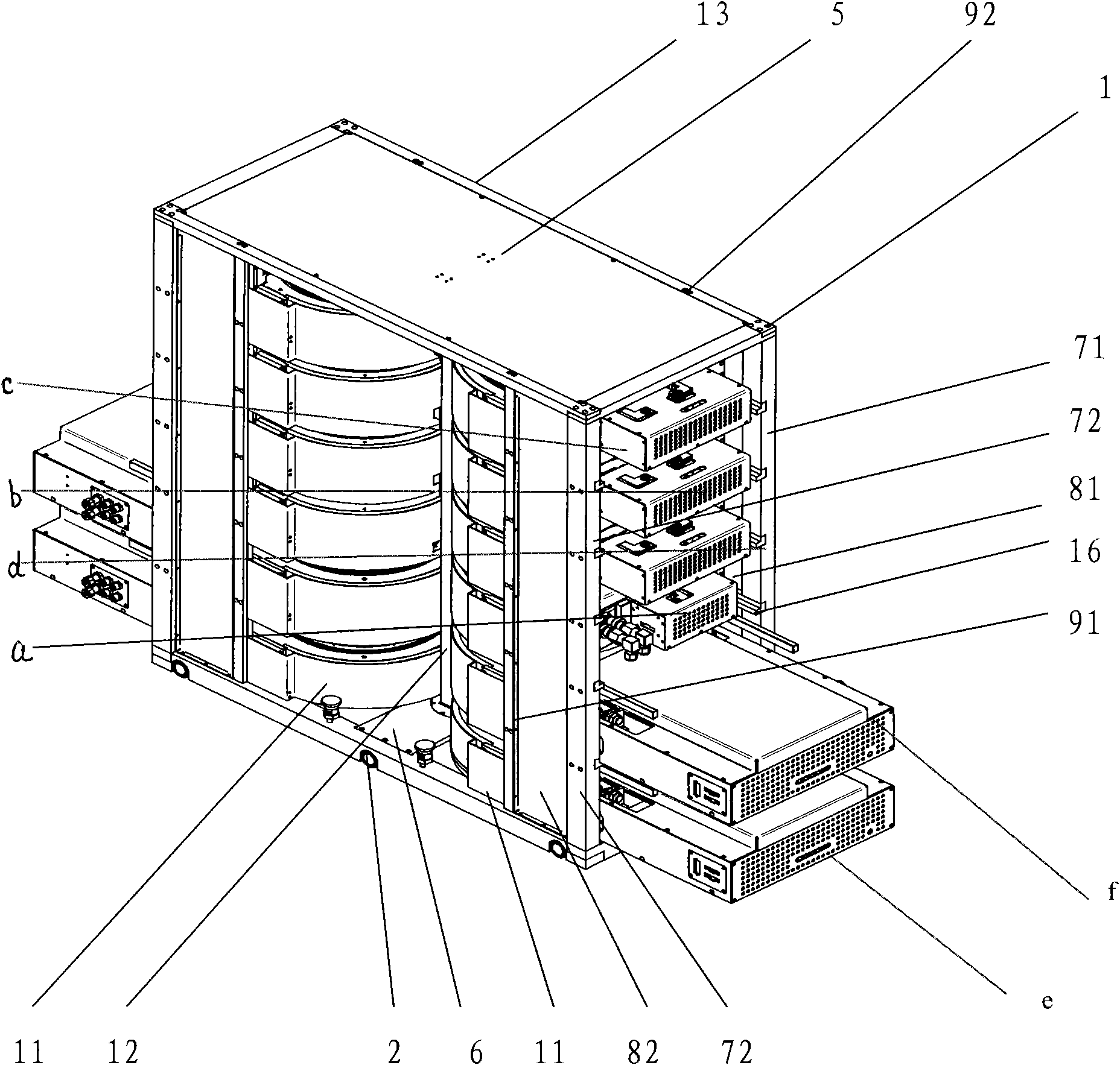
[0020] Embodiment: This example is described by taking a single process wall mode as an example. Such as figure 2 As shown, the process wall 3 is two walls with the same shape and structure, and the process units are arranged parallel and side by side. Each unit of the process wall has a wafer import and export port, and the wafer import and export port is arc-shaped transparent type structure; the arc-shaped inlet and outlet ends of the two walls are placed opposite to each other. The process robot 4 and the box station robot 2 are located on both sides of the wafer inlet and outlet of the process wall 3, and can take out or put wafers in the process wall 3 at the same time.

[0021] In order to facilitate the installation of the process wall in the frame of the complete equipment, the process wall of the present invention is installed in the frame of the process wall. The specific structure is as follows image 3 As shown: the frame of the process wall in this example is ...


PUM


Abstract

The invention discloses a process wall for glue spreading development equipment, which belongs to the technical field of glue spreading development of semiconductor wafers. Various process units of the process wall are parallelly arranged; the units of the process wall are provided with a wafer inlet and outlet end respectively; and the wafer inlet and outlet end has an arc-shaped run-through structure. The process wall has the advantages that the arc-shaped structures of inlets and outlets of the units of the process wall ensure that the wafer transmission forms a process mode of permeation transmission, break through the prior wafer transmission mode of the glue spreading development equipment, reduce the bottleneck in a wafer transmission path, also reduce the working position of a robot of a process section, and ensure that the effective utilization rate of the process units of the whole process wall is improved. The process wall meets the production requirement of a large-scale and high-productivity glue spreading development process. The application of the structural equipment has small land occupation area, and effectively reduces the pollution of the environment to wafers during the transmission; and the investment cost for the equipment is effectively reduced, and the production efficiency is improved.

Description

technical field [0001] The invention belongs to the technical field of gluing and development of semiconductor wafers, in particular to a process wall for gluing and developing process equipment for uniformly distributing photoresist and photoresist patterns on a semiconductor wafer. Background technique [0002] At present, the technologically advanced gluing and developing TRACK equipment is mainly composed of three blocks: loading and unloading block, process block 1, process block 2, and interface block. Station robot (or CS-R), frame body, etc.; the process modules contained in process block 1 and process block 2 are different, and the process modules mainly include coating units (or COT / BAC / TAC) and / or or development unit (or DEV), process robot (or PS-R), process heat treatment tower (or OVEN RACK), frame, etc., and the process heat treatment tower is loaded with cold plate (or CP), hot plate ( Or called HP and HHP), thickening unit (or called AD), cold and hot compo...

Claims


Application Information

Patent Timeline
Patent Type & Authority Applications(China)
IPC IPC(8): H01L21/00H01L21/677G03F7/00
Inventor 魏猛
Owner SHENYANG KINGSEMI CO LTD
Learn More