
Method for manufacturing printed wiring board

A technology for printed circuit boards and manufacturing methods, which is applied in the fields of printed circuit manufacturing, multilayer circuit manufacturing, printed circuit, etc., can solve problems such as increased workload and troublesome manufacturing of printed circuit boards, and achieve a sudden reduction in the number of processes, quick and easy results

Active Publication Date: 2009-12-16
ALPS ALPINE CO LTD +1
View PDF1 Cites 0 Cited by
  • Summary
  • Abstract
  • Description
  • Claims
  • Application Information

AI Technical Summary

Problems solved by technology

Therefore, there are problems such as that it is very troublesome to manufacture printed circuit boards, and the burden of work is increased.

Method used


Image

  • Method for manufacturing printed wiring board
  • Method for manufacturing printed wiring board
  • Method for manufacturing printed wiring board

Examples


Embodiment approach

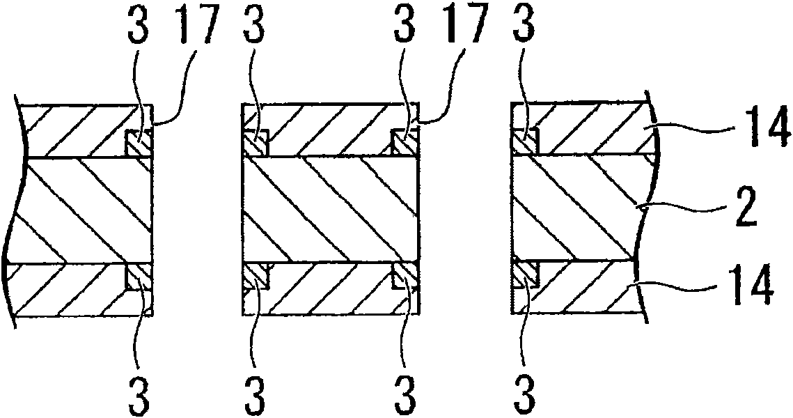
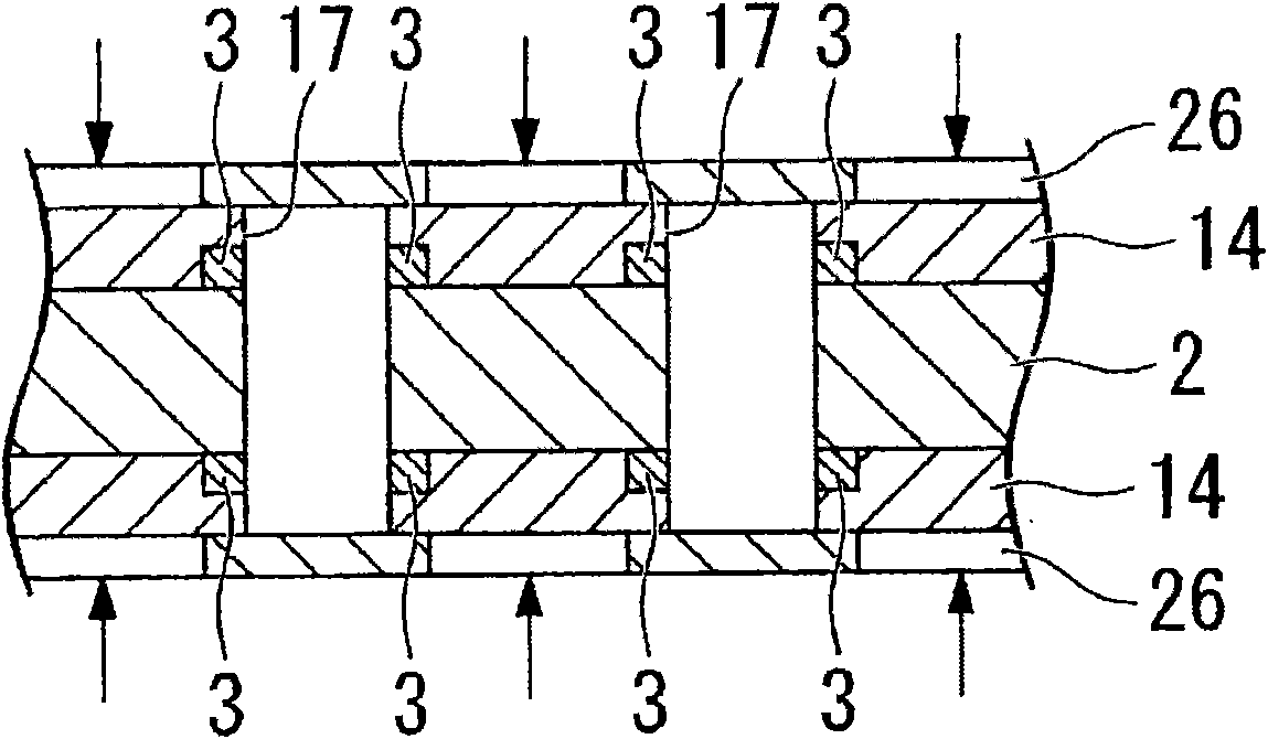
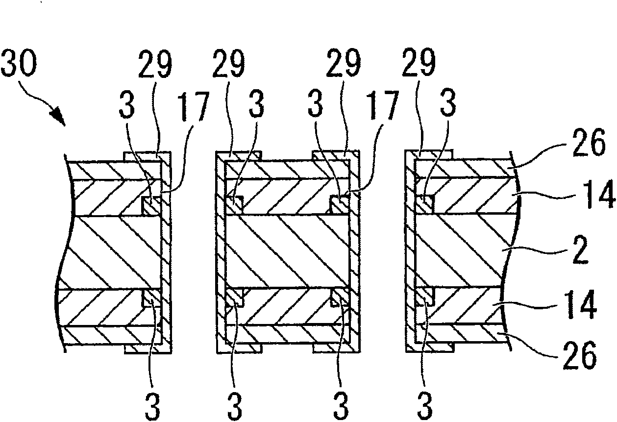
[0067] Next, an example of the following embodiments of the present invention will be described. In this embodiment, a method of manufacturing a printed wiring board having through holes will be described with reference to the drawings.

[0068] In the manufacturing method of the printed wiring board of the present embodiment, first, as Figure 6 As shown, prepare the existing copper clad laminate 4 . Next, since in this embodiment mode is formed as Figure 14 The steps before the shown through-hole 17 are the same as the conventional steps, and therefore description thereof will be omitted.

[0069] Such as Figure 14 As shown, it is assumed that the via hole 17 is formed through a via hole forming step.

[0070] Such as figure 1 As shown, in this embodiment, the etching step is provided before or after the via hole forming step. In this etching step, copper foil 15 is removed by etching. Then, in the degreasing process, the whole is degreased. Thus, if Figure 5 As ...


PUM


Abstract

Provided is a method for manufacturing printed wiring boards, by which the printed wiring boards can be quickly and easily obtained. The method is provided with a degreasing step of degreasing a substrate section; a step of irradiating the substrate section, which has been degreased in the degreasing step, with ultraviolet in an area equivalent to a position where no conductive pattern is to be formed; a catalyst adhering step of adhering a catalyst on the substrate section after ultraviolet irradiation; and a plating step of plating the substrate section whereupon the catalyst has been adhered in the catalyst adhering step.

Description

technical field [0001] The present invention relates to a method of manufacturing a printed wiring board mounted with various electronic components. Background technique [0002] Various printed wiring boards mounted with various electronic components and installed in electronic equipment have been used conventionally (for example, refer to Patent Document 1). [0003] Among these printed wiring boards, a printed wiring board having through holes is generally manufactured through the following steps. [0004] First, if Figure 6 As shown, a copper clad laminate 4 in which copper foil 3 is provided on both main surfaces of a substrate portion (substrate body) 2 made of epoxy resin or the like is prepared. Then, if Figure 7 As shown, a thin film 8 is provided on both surfaces of the copper foil 3 . [0005] further, such as Figure 8 As shown, a pattern film 9 for forming a conductor pattern is provided on both surfaces of the film 8 . Then, in an exposure step, ultravio...

Claims


Application Information

Patent Timeline
IPC IPC(8): H05K3/18
CPCH05K3/429H05K3/185H05K3/426H05K3/4661H05K3/46
Inventor 佐藤一小原一夫田口好弘森邦夫村上秀俊
Owner ALPS ALPINE CO LTD
Learn More