Method for reducing gate induced drain leakage current in N-channel metal oxide semiconductor (NMOS) devices
A leakage current and device technology, used in semiconductor/solid-state device manufacturing, circuits, electrical components, etc., can solve serious problems and achieve the effect of reducing GIDL, reducing tunneling current, and improving GIDL effect
- Summary
- Abstract
- Description
- Claims
- Application Information
AI Technical Summary
Problems solved by technology
Method used
Image

Examples
Embodiment Construction
[0023] The specific embodiments of the present invention will be described in detail below in conjunction with the accompanying drawings.
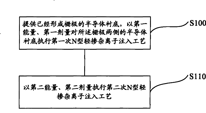
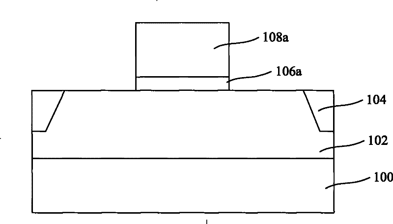
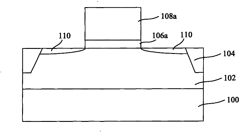
[0024] The invention provides a method for reducing the GIDL of an NMOS device. The LDD doped region of the NMOS device is formed by performing two or more lightly doped ion implantation processes, and as the number of times increases, the depth of the implantation increases. The concentration decreases; or as the number of times increases, the depth of implantation gradually decreases and the concentration increases; through the implantation of lightly doped ions with a higher concentration and a shallower depth, the underside of the gate caused by the gate bias voltage is reduced. The size of the depletion layer in the LDD region to improve the GIDL effect, and to reduce the concentration gradient of impurity ions between the formed LDD doped region and the pocket doped region by implanting lightly doped ions with a lower concentration an...
PUM
 Abstract
Description
Claims
Application Information
 - R&D
- Intellectual Property
- Life Sciences
- Materials
- Tech Scout
- Unparalleled Data Quality
- Higher Quality Content
- 60% Fewer Hallucinations
Browse by: Latest US Patents, China's latest patents, Technical Efficacy Thesaurus, Application Domain, Technology Topic, Popular Technical Reports.
© 2025 PatSnap. All rights reserved.Legal|Privacy policy|Modern Slavery Act Transparency Statement|Sitemap|About US| Contact US: help@patsnap.com