
Chip with drive integrated circuit and corresponding liquid crystal display

A technology for driving integrated circuits and liquid crystal displays, which can be used in circuits, electrical solid-state devices, instruments, etc., to solve problems such as poor bump indentation of driver chips, expensive conductive particles, and poor display screen display.

Active Publication Date: 2012-03-14
HANNSTAR DISPLAY CORPORATION
View PDF2 Cites 0 Cited by
  • Summary
  • Abstract
  • Description
  • Claims
  • Application Information

AI Technical Summary

Problems solved by technology

However, since the conductive particles themselves are relatively expensive, the cost of displays fabricated by the ACF process cannot be effectively reduced.
On the other hand, if NCF is directly used to bond the existing driver chip and the glass substrate of the display, the problem of poor bump indentation of the driver chip will easily occur, resulting in poor display of the display screen.
This is because NCF itself does not have the function of conducting electricity, and it is not suitable for filling the gap between the bump and the wire to eliminate the gap, so not all driver chips are suitable for bonding using the NCF process

Method used


Image

  • Chip with drive integrated circuit and corresponding liquid crystal display
  • Chip with drive integrated circuit and corresponding liquid crystal display
  • Chip with drive integrated circuit and corresponding liquid crystal display

Examples


Embodiment Construction

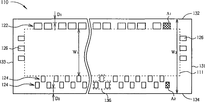
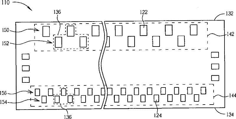
[0010] The present invention provides a display driver chip suitable for COG packaging technology, wherein the area distribution of the bumps on the opposite two edges of the chip is uniform (the total area ratio of the upper edge bumps to the lower edge bumps is about 0.8 to 1.2), so It can improve the problem of poor indentation at the input end and output end. The bump layout of the present invention can be applied to any integrated circuit device, especially a driving chip of a liquid crystal display, such as a source driving chip (source driving chip or source driving IC) listed on the X-axis or a gate driver listed on the Y-axis Chip (gate driving chip or gate driving IC).

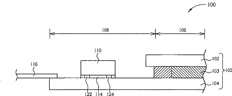
[0011] figure 1 A schematic cross-sectional view of a liquid crystal display 100 showing a first preferred embodiment of the present invention, and figure 2 A schematic structural diagram showing a chip 110 with a driver integrated circuit according to the first preferred embodiment of the present...


PUM


Abstract

The invention relates to a chip with a drive integrated circuit and a corresponding liquid crystal display. The invention provides a projection layout of the chip, which is suitable for the packaging technology of the chip on glass. The chip with the drive integrated circuit comprises a plurality of first projections and a plurality of second projections and can be electrically connected to the glass substrate of the liquid crystal display, wherein the first projections and the second projections are arranged on the surface of the chip and respectively adjacent to two opposite long edges of the chip, and the total area ratio of the first projections to the second projections ranges from 0.8 to 1.2. Thus, when the chip and the glass substrate of the liquid crystal display are jointed, pressure can be uniformly distributed on each position of the chip so that the jointed stability of the chip is improved.

Description

technical field [0001] The invention provides a chip with a driving integrated circuit, especially a chip applicable to chip on glass (chip on glass, COG) packaging technology. Background technique [0002] COG packaging technology is to install the driving chip (generally or called the driving IC, the driving chip usually has an integrated circuit) directly on the glass substrate of the display to output the required voltage or signal to the display pixels, and then control The degree of twist of the liquid crystal molecules or the color of the pixel. Among them, the COG process can connect the driving chip and the lower glass substrate of the display through anisotropic conductive film (anisotropic conductive film, ACF) or non-conductive film (non-conductive film, NCF), so that the output end / input end of the driving chip Bumps (input / output bumps) can be electrically connected to metal traces on the surface of the lower glass substrate. [0003] ACF is generally compose...

Claims


Application Information

Patent Timeline
Patent Type & Authority Patents(China)
IPC IPC(8): H01L23/485G02F1/13
CPCH01L2924/0002
Inventor 汤宝云孙伟豪
Owner HANNSTAR DISPLAY CORPORATION
Learn More