
Driver chip and display device

A technology for driving chips and display devices, used in semiconductor/solid-state device parts, semiconductor devices, electrical components, etc., can solve problems such as overvoltage of conductive particles, and achieve the effect of avoiding bad indentation

Inactive Publication Date: 2015-03-04
HEFEI BOE OPTOELECTRONICS TECH +1
View PDF4 Cites 6 Cited by
  • Summary
  • Abstract
  • Description
  • Claims
  • Application Information

AI Technical Summary

Problems solved by technology

During the bonding process, when the driving chip is subjected to a large pressure, the two ends of the driving chip are deformed too much, and the conductive particles in the opposite-sex conductive film on the output terminal / output terminal bump at both ends of the bump column have a risk of overvoltage
After the pressure is removed, the driver chip will restore its shape, resulting in the undesirable phenomenon that the indentation at both ends is shallow and the indentation in the middle is deep

Method used


Image

  • Driver chip and display device
  • Driver chip and display device
  • Driver chip and display device

Examples


Embodiment 1

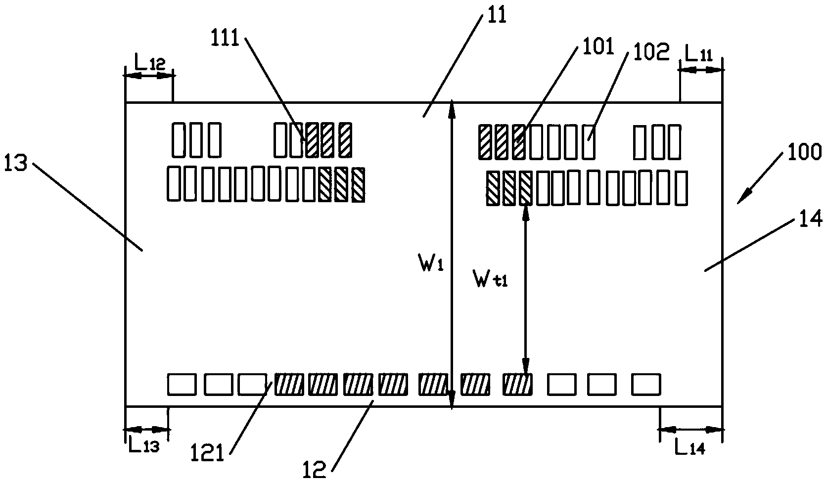
[0031] refer to figure 2 As shown, the driving chip 100 of this embodiment is a source driving chip (source driving chip or source driving IC), and the surface of the driving chip 100 has a first edge 11, a second edge 12, and a third edge 13 opposite to each other. and the fourth edge 14 , the third edge 13 and the fourth edge 14 intersect with the first edge 11 and the second edge 12 . Preferably, the first edge 11 and the second edge 12 are parallel to each other, the third edge 13 and the fourth edge 14 are parallel to each other, and the driving chip 100 has a rectangular structure. The driving chip 100 includes: a plurality of connecting bumps 101 and a plurality of supporting bumps 102 . A plurality of connecting bumps 101 and supporting bumps 102 are arranged along the first edge 11 of the driver chip 100 to form at least one first bump row 111, the first bump row 111 in this embodiment is two rows, each row There is at least one supporting bump 102 at both ends of ...

Embodiment 2

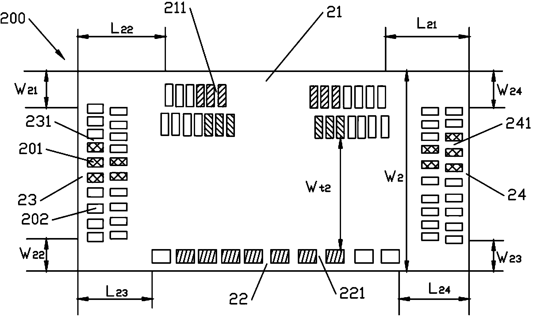
[0034] refer to image 3As shown, the driving chip 200 of this embodiment is a gate driving chip (gate driving chip or gate driving IC), and the driving chip 200 has a rectangular structure. The surface of the driver chip 200 has a first edge 21 , a second edge 22 , a third edge 23 , and a fourth edge 24 opposite to each other; the third edge 23 and the fourth edge 24 intersect with the first edge 21 and the second edge 22 . Preferably, the first edge 21 and the second edge 22 are parallel to each other, the third edge 23 and the fourth edge 24 are parallel to each other, and the driving chip 200 has a rectangular structure. The driving chip 200 includes: a plurality of connecting bumps 201 and a plurality of supporting bumps 202 . A plurality of connecting bumps 201 and supporting bumps 202 are arranged along the first edge 21 of the driver chip 200 to form at least one first bump row 211, the first bump row 211 in this embodiment is two rows, each row There is at least one...


PUM


Abstract

The invention, which relates to the technical field of a display driver chip, discloses a driver chip. The surface of the driver chip has a first edge and a second edge, wherein the two edges are opposite to each other. The driver chip is characterized in that connecting projection blocks and support projection blocks are distributed along the first edge to form at least one first projection block column, wherein at least one support projection block is respectively arranged at each of two ends of the first projection block column; the connecting projection blocks and the support projection blocks are distributed along the second edge to form at least one second projection block column, wherein at least one support projection block is respectively arranged at each of two ends of the second projection block column. According to the invention, the projection block columns are arranged at the surface of the driver chip and the support projection blocks are arranged at the end portions of the projection block columns, so that the driver chip can be well supported. During bonding and packaging, the whole driver chip can bear the forces in a balanced mode, thereby avoiding a poor indentation phenomenon. In addition, the invention also provides a display device having the driver chip.

Description

technical field [0001] The invention relates to the technical field of display device driving chips, in particular to a driving chip and a display device. Background technique [0002] COG packaging technology is to install the driving chip (generally or called the driving IC, the driving chip usually has an integrated circuit) directly on the lower glass substrate of the display to output the required voltage or signal to the display pixels, and then Control the twist degree of liquid crystal molecules or pixel color. In the COG packaging technology, multiple output / input bumps (input / output bumps) are arranged on the surface of the driver chip, and through anisotropic conductive film (anisotropic conductive film, ACF) or non-conductive film (non- The conductive film (NCF) electrically connects the driving chip and the metal trace on the lower glass substrate of the display. [0003] Such as figure 1 As shown, in the prior art, the driver chip 1 generally has a rectangul...

Claims


Application Information

Patent Timeline
Patent Type & Authority Applications(China)
IPC IPC(8): H01L23/488H01L23/58
CPCH01L2224/14133H01L24/14H01L2224/14135H01L2224/14132H01L2224/14177H01L2924/3511H01L2924/15788H01L24/17H01L2924/12041
Inventor 程亮齐鹏郑璐
Owner HEFEI BOE OPTOELECTRONICS TECH
Learn More