Creasing inspection device and method thereof

A technology of inspection device and indentation, applied in the direction of measuring device, instrument, electrical components, etc., can solve problems such as difficult inspection

Inactive Publication Date: 2012-12-12
ウィンテックカンパニーリミテッド
View PDF3 Cites 0 Cited by
  • Summary
  • Abstract
  • Description
  • Claims
  • Application Information

AI Technical Summary

Problems solved by technology

However, it is difficult to quickly and accurately inspect each indentation 8 produced by the conductive particles 6 in the micron unit

Method used


Image

  • Creasing inspection device and method thereof
  • Creasing inspection device and method thereof
  • Creasing inspection device and method thereof

Examples


Embodiment Construction

[0026] Hereinafter, an indentation inspection device and a method thereof according to preferred embodiments of the present invention are explained with reference to the accompanying drawings.

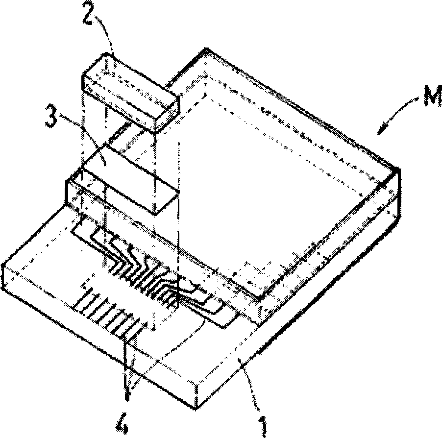
[0027] Take, for example, a flat panel display panel employing only a COG method among various wireless bonding methods including chip-on-glass (COG), chip-on-film (COF), flexible printed circuit board (FPC), and tape carrier package (TCP).

[0028] Therefore, the substrate to be inspected is a glass substrate.

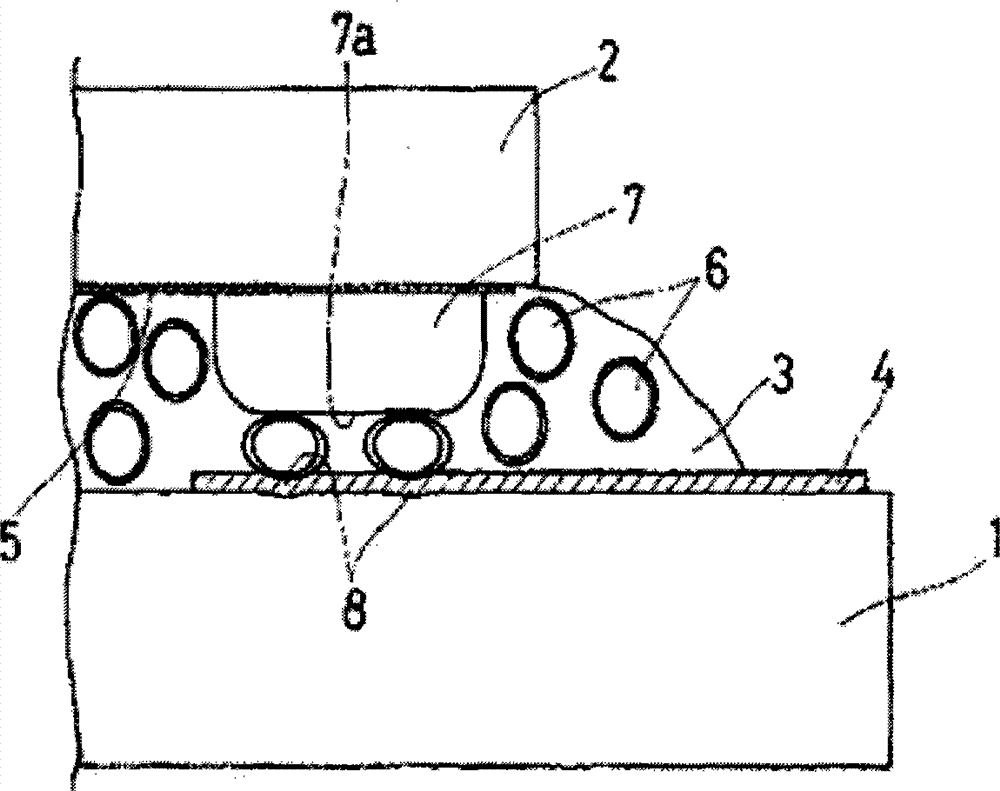
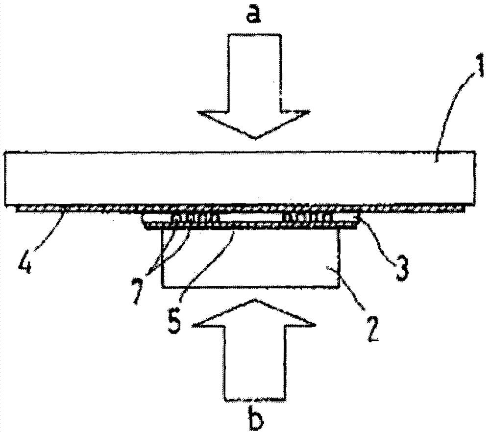
[0029] Figure 4 It is a configuration diagram schematically showing an indentation inspection device according to the present invention. Figure 5 is a block diagram showing an inspection portion of an indentation inspection device according to the present invention. Figure 6 A method for selecting the inspection area of ​​the indentation inspection device according to the present invention is schematically shown. Figure 7 A method for inspecting indentations by the inde...


PUM


Abstract

The invention relates to a creasing inspection device and method thereof, more particularly, a creasing inspection device and method for selecting a check area for creasing inspection rapidly and precisely, and judge the existence of normal creasing rapidly and precisely. Hence, according to the invention, the creasing inspection device comprises the following components: a workstation for fixinga cardinal plate with creasing on it; a microscope above the workstation for observing lower side of the cardinal plate; a camera connected with the microscope for obtaining image data observed by lower side of the cardinal plate of the microscope; a inspection area selecting part for receiving the obtained image data from the camera to select creasing inspection area for creasing inspection fromthe obtained image data; and a creasing detection part for detecting brightness distribution information in each detection area of each detection area that has a boundary with scheduled shape in the inspection area, so as to detect creasing index according to the detected brightness distribution information.

Description

technical field [0001] The invention relates to an indentation inspection device and method thereof. More particularly, the present invention relates to an indentation inspection device and method thereof for quickly and accurately selecting an inspection area for indentation inspection, and for quickly and accurately determining whether there is a normal indentation. Background technique [0002] Wire-free bonding technologies such as Chip-on-Glass (COG), Chip-on-Film (COF), Flexible Printed Circuit Board (FPC), and Tape Carrier Package (TCP) types are used in recent flat panel display devices, and these technologies also For wireless phones, personal digital assistants (PDA) and display devices, etc. [0003] For example figure 1 as shown, figure 1 Depicting a COG type, a flat panel display device M includes a glass substrate 1 on which a panel electrode 4 including a plurality of indium tin oxide ITO electrodes is formed, and a semiconductor chip 2 (or driver chip) mou...

Claims


Application Information

Patent Timeline
Patent Type & Authority Patents(China)
IPC IPC(8): G01N21/956
CPCH01L2224/73204G02F1/13G02F1/1345
Inventor 许玟硕孙暎卓
Owner ウィンテックカンパニーリミテッド
Why Eureka
Try Eureka