PCB-type traveling wave sensor
A traveling wave sensor and induction line technology, applied in the fault location and other directions, can solve the problems of low anti-interference ability and low precision, and achieve the effect of high transient stability, sensitive reflection and high linearity
- Summary
- Abstract
- Description
- Claims
- Application Information
AI Technical Summary
Problems solved by technology
Method used
Image
Examples
Embodiment Construction
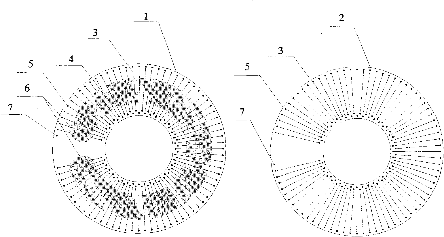
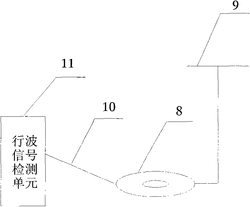
[0011] see figure 1 , the PCB traveling wave sensor consists of an upper panel (1) and a lower panel (2), and the upper panel (1) includes: a secondary induction coil (3), a primary flow loop (4), a through hole (5), A primary signal port (6) and a secondary coil output terminal (7); the lower panel (2) includes: a secondary induction coil (3), a through hole (5) and a secondary coil output terminal (7). In the PCB type, the inner ring through holes are staggered and arranged in two rows. When a transient traveling wave signal is input into the primary signal interface (6), a sudden change current is generated in the primary flow loop (4), and a sudden change signal is induced in the secondary induction coil (3), and at the same time, the secondary line is perpendicular to The direction of the PCB type generates an electromagnetic field, and the electromagnetic fields generated by the secondary lines in the upper panel and the lower panel are equal in size and opposite in dir...
PUM
 Abstract
Description
Claims
Application Information
 - R&D Engineer
- R&D Manager
- IP Professional
- Industry Leading Data Capabilities
- Powerful AI technology
- Patent DNA Extraction
Browse by: Latest US Patents, China's latest patents, Technical Efficacy Thesaurus, Application Domain, Technology Topic, Popular Technical Reports.
© 2024 PatSnap. All rights reserved.Legal|Privacy policy|Modern Slavery Act Transparency Statement|Sitemap|About US| Contact US: help@patsnap.com


