Supercharge Your Innovation With Domain-Expert AI Agents!

Packaging process of light-emitting elements

A light-emitting element and packaging process technology, which is applied in the direction of electrical components, semiconductor/solid-state device manufacturing, and electric solid-state devices, to achieve the effects of improving luminous efficiency, increasing production capacity, and reducing manufacturing costs

Inactive Publication Date: 2011-11-30
LIUNG FENG INDAL
View PDF6 Cites 0 Cited by
  • Summary
  • Abstract
  • Description
  • Claims
  • Application Information

AI Technical Summary

Problems solved by technology

[0003] Furthermore, in the structure of the existing light-emitting element, the light-emitting diode chip is bonded by the bonding material, so the heat conduction will be limited between the layers Factors such as the contact interface of each layer and the different thermal conductivity coefficients of each layer directly affect the luminous performance and working life of the light-emitting element, and the light emitted by the light-emitting element can only directly pass through the filling material to the outside, and a small part passes through the side of the concave part. Reflection passes through the filler material to the outside world, therefore, the luminous efficiency is not as expected

Method used


Image

  • Packaging process of light-emitting elements
  • Packaging process of light-emitting elements
  • Packaging process of light-emitting elements

Examples


no. 1 example

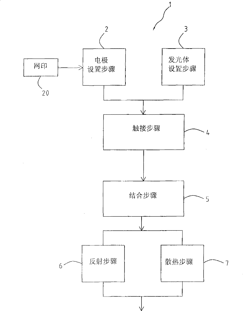
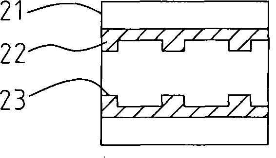
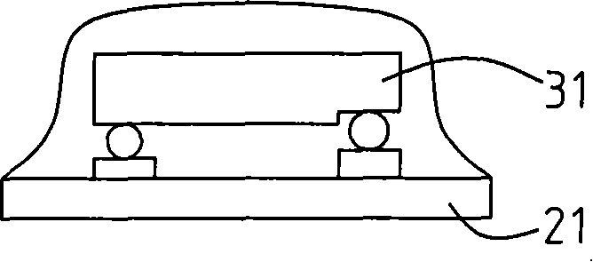
[0023] refer to Figure 2A -F is the first embodiment of the packaging process of the light-emitting element of the present invention. In this embodiment, a positive electrode 22 and a negative electrode 23 are defined by etching on a carrier 21, so that the carrier 21 is formed with a positive electrode and a negative electrode. electrode slides (i.e. step 2 for electrode setup, see Figure 2A and Figure 2B ; As previously mentioned, the material of the positive electrode and the negative electrode can also be directly selected to directly define the electrode, or the electrode carrier with the positive electrode and the negative electrode can be selected without going through the etching process), in addition, Select a surface-mounted (SMD) light-emitting diode chip 31 with a positive electrode 32 and a negative electrode 33 on it (that is, the step 3 for setting the light emitter), and then use ball grid array packaging technology (BGA) to define a positive electrode 22 ...


PUM


Abstract

The invention relates to a package process of a light emitting element, comprising: an electrode setting step, an illuminant setting step, a contact step and a combining step. In the electrode setting step, a anode and a cathode are defined; in the illuminant setting step, a light emitting diode wafer having an anode and a cathode is used as an illuminant ; in the contact step, the defined anode and the cathode as well as the anode and the cathode on the light emitting diode wafer are communicated and combined into a whole; and in the combining step, the defined anode and the cathode and the light emitting diode wafer are tightly combined into a whole. In the package process of the light emitting element, the electrode of the light emitting diode wafer can be communicated with an outside electrode in advance, thereby work for assembling posterior-segment products can be simplified, the productivity can be increased, and the production cost can be reduced.

Description

technical field [0001] The present invention relates to a packaging process of a light-emitting element, in particular to a process for manufacturing a light-emitting element with a light-emitting diode chip. The method can increase production capacity and reduce manufacturing costs, and can make the manufactured light-emitting element The luminous efficiency is improved. Background technique [0002] In the production of light-emitting elements with light-emitting diode chips, the light-emitting diode chip is firstly manufactured, and then the light-emitting diode chip is bonded in the base with a concave portion by the bonding material, and the light-emitting diode chip is fixed by the filling material. When the concave portion is filled, the fabrication of the light-emitting element is completed. However, the light-emitting diode chip must be electrically connected to the external circuit through the electrodes on it to be able to emit light. Therefore, in the manufactu...

Claims


Application Information

Patent Timeline
Patent Type & Authority Patents(China)
IPC IPC(8): H01L33/00H01L21/60H01L23/488
CPCH01L2224/16225H01L24/17H01L2224/48227H01L2224/48091H01L2224/17H01L2924/12041H01L2924/00014H01L2924/00H01L2924/00012
Inventor 许苍林林恒毅
Owner LIUNG FENG INDAL
Features
  • R&D
  • Intellectual Property
  • Life Sciences
  • Materials
  • Tech Scout
  • Unparalleled Data Quality
  • Higher Quality Content
  • 60% Fewer Hallucinations
Learn More