Method for packaging semiconductor with cavity

A packaging method and semiconductor technology, which are applied in the fields of semiconductor devices, semiconductor/solid-state device manufacturing, electric solid-state devices, etc., can solve problems such as difficulty in uniformly coating barrier layers, unstable physical properties, and contamination of chips.

Inactive Publication Date: 2009-09-30
LINGSEN PRECISION INDS
View PDF0 Cites 0 Cited by
  • Summary
  • Abstract
  • Description
  • Claims
  • Application Information

AI Technical Summary

Problems solved by technology

[0003] However, in these conventional micro-electromechanical chip packaging processes with chambers, since the adhesive is gel-like and has unstable physical properties, it is difficult to evenly coat the wall-like barrier layer, and then coat the adhesive on the barrier layer. And after the cover is put on, there are occasional cases where the glue overflows ...

Method used


Image

  • Method for packaging semiconductor with cavity
  • Method for packaging semiconductor with cavity
  • Method for packaging semiconductor with cavity

Examples


Embodiment Construction

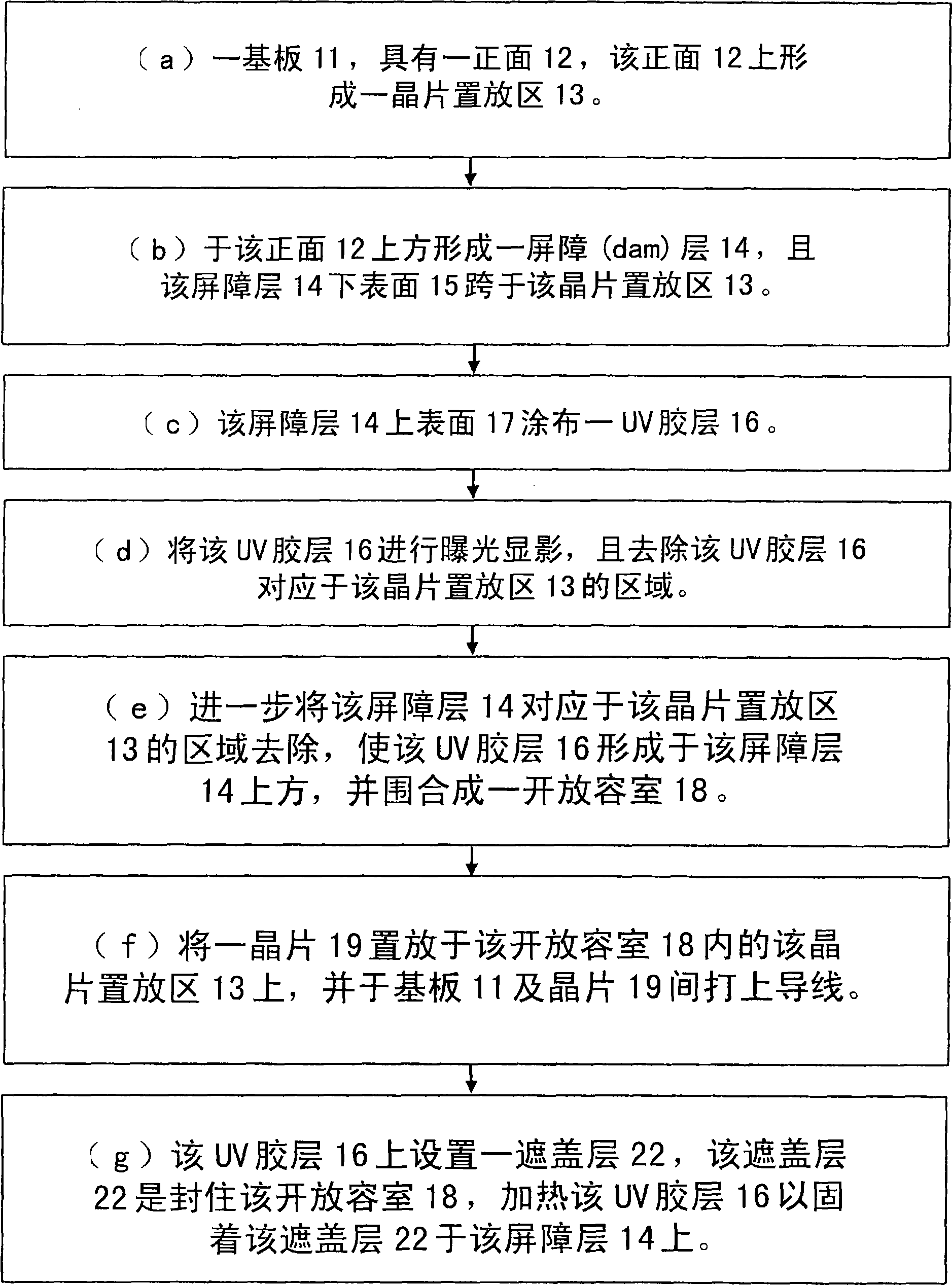
[0038] In order to describe in detail the steps and flow characteristics of the present invention, the following preferred embodiment is given and described as follows in conjunction with the accompanying drawings, wherein:

[0039] figure 1 It is an action flowchart of a preferred embodiment of the present invention;

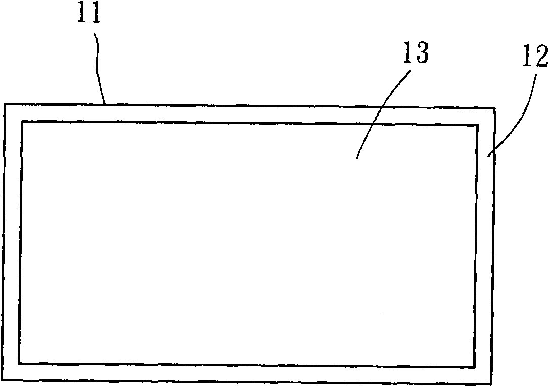
[0040] Figure 2 (A) is a schematic diagram of a preferred implementation step of the present invention, which shows the configuration of the chip placement area on the substrate;

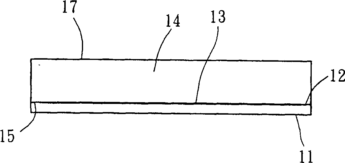
[0041] FIG. 2(B) is a schematic diagram of a preferred implementation step of the present invention, which shows the appearance of the substrate and the barrier layer when they are stacked;

[0042] Fig. 2 (C) is a schematic diagram of a preferred implementation step of the present invention, which has shown the pattern of coating UV adhesive layer above the barrier layer;

[0043] Fig. 2 (D) is a schematic diagram of a preferred implementation step of the present invention, which ...


PUM


Abstract

The invention relates to a method for packaging a semiconductor with a cavity, which comprises the following steps of: a, providing a substrate of which the front side has a chip accommodating area; b, forming a barrier layer above the front side; c, coating a UV adhesive layer on the upper surface of the barrier layer; d, removing an area, corresponding to the chip accommodating area, in the UV adhesive layer; e, further removing an area, corresponding to the chip accommodating area, in the barrier layer; f, arranging a chip on the chip accommodating area in an open accommodating chamber and molding an wire on the chip to electrically connect the chip and the substrate; and g, arranging a cover layer on the UV adhesive layer and heating the UV adhesive layer to fix the cover layer on the barrier layer. The design of the invention can reduce glue overflow generated during the packaging of the semiconductor considerably; and the method can be implemented by the prior art without increasing equipment purchase cost.

Description

technical field [0001] The present invention relates to semiconductor packaging, in particular to an improved method for semiconductor packaging steps. Background technique [0002] Known packaging components with chambers, such as: micro-electromechanical chip packaging or CMOS chip packaging methods are mostly to first stick the chip on the chip placement area of ​​a substrate, and build a wall-shaped surrounding the chip placement area. Barrier layer (dam), the bottom surface of the barrier layer is bonded to the periphery of the substrate placement area to enclose the chip in the middle, then electrically connect the chip and the substrate, and finally coat the upper surface of the barrier layer with adhesive, and then seal the A cover, such as glass, etc., is pasted on the barrier layer to package the chip in a closed space. [0003] However, in these conventional micro-electromechanical chip packaging processes with chambers, since the adhesive is gel-like and has uns...

Claims


Application Information

Patent Timeline
IPC IPC(8): H01L21/50H01L21/52
CPCH01L2224/48091H01L2924/16195H01L2924/00014
Inventor 叶崇茂
Owner LINGSEN PRECISION INDS
Why Eureka
Try Eureka