Die bonding method for automatic quartz alignment by image recognition

An automatic image and die-bonding technology, applied in semiconductor/solid-state device manufacturing, electrical components, comprehensive factory control, etc., can solve the problems of die-bonding accuracy and speed constraints, poor stability, low efficiency of artificial die-bonding, etc. The effect of high efficiency, cost saving, and improvement of die bonding speed and precision

Inactive Publication Date: 2011-01-12
NANCHANG HANGKONG UNIVERSITY
View PDF0 Cites 0 Cited by
  • Summary
  • Abstract
  • Description
  • Claims
  • Application Information

AI Technical Summary

Problems solved by technology

At present, there are two well-known crystal bonding methods at home and abroad: one is artificial crystal bonding under a microscope, which is inefficient; the other is to use automatic crystal bonding machines to automatically bond crystals
The working principle of various automatic die bonding machines is to use the Bangtou to take the crystal and then move to the bonding position for die bonding. Although the structure of the Bangtou system is different, it is far from the crystal picking position to the bonding position. Distance movement, crystal bonding accuracy and speed are severely restricted, and various auxiliary motion mechanisms are complex in structure and poor in stability

Method used


Image

  • Die bonding method for automatic quartz alignment by image recognition
  • Die bonding method for automatic quartz alignment by image recognition

Examples


Embodiment Construction

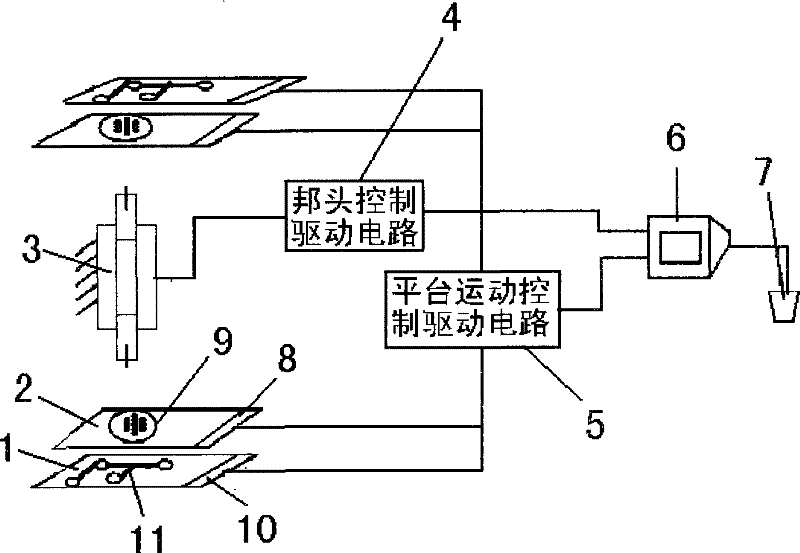
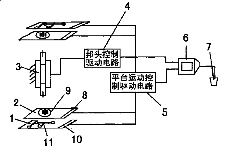
[0015] First, adjust the wafer platform fixture and circuit board platform fixture to an appropriate distance according to the height of the wafer, so that the distance from the wafer film to the circuit board solid point is slightly greater than the height of the wafer, and then respectively fix the wafer and the circuit board in the same group. On the wafer platform fixture and the circuit board platform fixture, and glue the end of the wafer to prepare for solid crystal, use the camera to take pictures of the wafer platform fixture and the circuit board platform fixture respectively, input the image data into the computer, and the computer Analyze, calculate and process the captured image, so that the wafers on the wafer ring and the corresponding die-bonding positions on the circuit board are automatically matched one by one, and the coordinate deviation value of each corresponding point is calculated. In order to have a calculation and analysis benchmark, Set a reference p...


PUM


Abstract

A high-speed die bond method for crystal by automatic image recognition is characterized in that the die bond method comprises the following steps: (1) a wafer platform and a circuit board platform realize driving in X and Y direction, the two platforms all select a Bonder Head position moving up and down as an origin of coordinate, all the origins automatically reset to zero when starting up; (2) image data are input into a computer which is responsible for analyzing, computing and processing the input images, the computer can process a plurality of groups of image data at the same time and match and compute the deviation of coordinates of corresponding points in each group based on the requirements; (3) movement to the place right under the Bonder Head or right above the Bonder Head is carried out according to the regulated time sequence, the wafer is pressed and mounted on the circuit board, thus completing die bond. The method has the advantages that the automatic position controlof computer is adopted, the Bonder Head does not need reciprocation, the die bond efficiency is high, a plurality of groups of die bond images can be processed simultaneously, the cost is saved and the requirement of improving the die bond speed and accuracy is met.

Description

technical field [0001] The invention relates to a high-speed crystal-bonding method, in particular to a high-speed crystal-bonding method for automatic image recognition alignment. Background technique [0002] With the increasingly urgent requirements for energy saving and emission reduction worldwide, the application of semiconductor lighting projects is becoming more and more extensive. At present, there are two known methods of die bonding at home and abroad: one is artificial die bonding under a microscope, which is inefficient; the other is automatic die bonding using an automatic die bonder. The working principle of various automatic die bonding machines is to use the Bangtou to take the crystal and then move to the bonding position for die bonding. Although the structure of the Bangtou system is different, it is far from the crystal picking position to the bonding position. Distance movement, crystal bonding accuracy and speed are severely restricted, and various au...

Claims


Application Information

Patent Timeline
Patent Type & Authority Patents(China)
IPC IPC(8): H01L33/00G05B19/418H01L21/68
Inventor 王云张绪坤储珺
Owner NANCHANG HANGKONG UNIVERSITY
Why Eureka
Try Eureka