
Wireless receiver and method for eliminating DC offset of wireless receiver

A wireless receiver and step size adjustment technology, applied in the direction of DC level restoration device/bias distortion correction, electrical components, transmission systems, etc., can solve problems such as useful signal damage, signal damage, nonlinear distortion, etc. The effect of mode offset cancellation

Inactive Publication Date: 2009-07-01
BEIJING LHWT MICROELECTRONICS
View PDF0 Cites 7 Cited by
  • Summary
  • Abstract
  • Description
  • Claims
  • Application Information

AI Technical Summary

Problems solved by technology

The disadvantage of using a high-pass filter is that it destroys the useful signal near zero frequency; and directly using a programmable current source or current sink to compensate the signal path may cause nonlinear distortion and damage the useful signal.

Method used


Image

  • Wireless receiver and method for eliminating DC offset of wireless receiver
  • Wireless receiver and method for eliminating DC offset of wireless receiver
  • Wireless receiver and method for eliminating DC offset of wireless receiver

Examples


Embodiment Construction

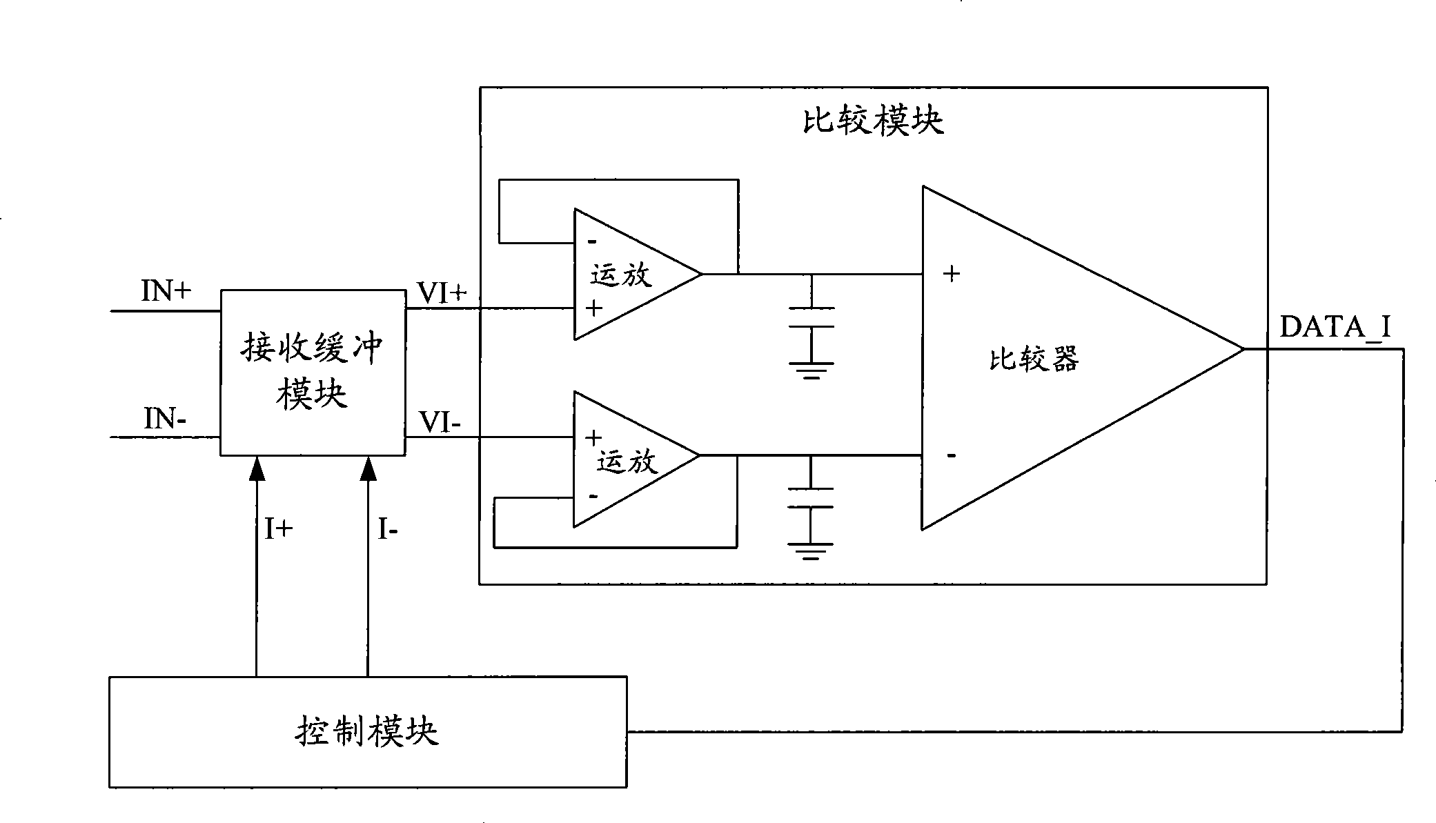
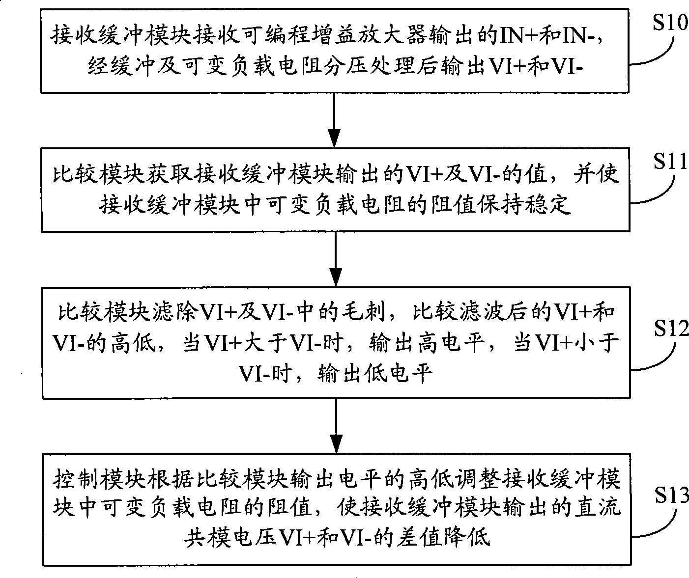
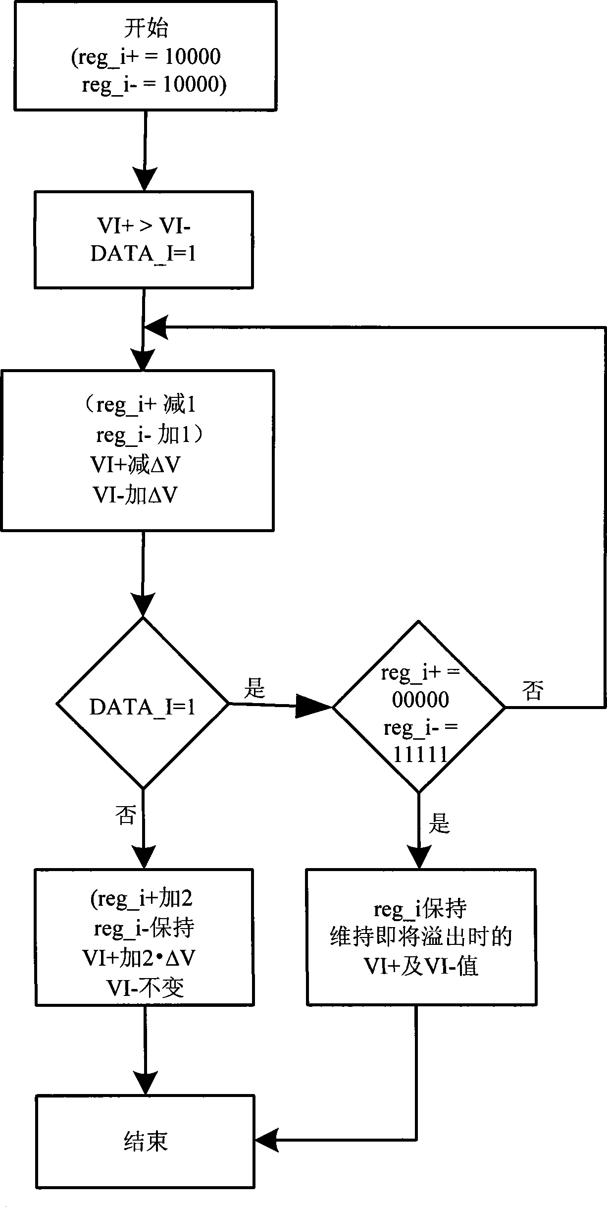
[0042] The present invention adopts the method of inserting a buffer circuit in the signal path to realize the elimination of the offset. Specifically, the buffer circuit is inserted in the signal link of the receiver that needs to eliminate the DC offset. The buffer circuit is a source follower structure. By buffering The compensation of the circuit realizes the calibration and elimination of the DC offset. The principle of compensating the buffer circuit and realizing DC offset elimination is to compare the level of the two common-mode output voltages, and then subtract ΔV from the potential of the higher voltage (ΔV is the adjustment step size), and the potential of the lower voltage Add ΔV, and then continue to compare, and use the successive approximation method to control the difference of the output common-mode voltage within ΔV, ΔV is the accuracy that can be achieved by calibration or compensation, thus realizing the calibration of the DC offset in the receiver and el...


PUM


Abstract

The invention discloses a wireless receiver and a method for eliminating the DC offset in the wireless receiver. The wireless receiver comprises a buffer module, a comparison module and a control module, wherein the buffer module is a part of the circuit of the wireless receiver and is used for receiving the outputs IN plus and IN minus from a prior programmable gain amplifier and outputting VI plus and VI minus to the input of the ADC in a baseband processing chip after buffing treatment and voltage division by a variable-load resistor; the comparison module is specifically used for calibration and is used for comparing the difference of the received outputs VI plus and VI minus from the buffer module, outputting the high electrical level when the VI plus is larger than the VI plus and outputting the low electrical level when the VI plus is smaller than the VI minus; and the control module regulates the resistance of the variable-load resistor in the buffer module according to the output level from the comparison module, so as to reduce the difference in DC common-mode voltage between the output VI plus and the output VI minus from the buffer module.

Description

technical field [0001] The invention relates to wireless receiver technology, in particular to a wireless receiver and a method for eliminating DC imbalance in the wireless receiver. Background technique [0002] In a zero-IF receiver, since the useful frequency band contains zero frequency, the DC offset of the analog baseband differential output DC common-mode voltage will damage the useful signal, and may saturate the subsequent circuit, affecting the processing of the signal by the subsequent circuit . This requires offset cancellation before the analog baseband output. [0003] DC offset is caused by device mismatch and process variation. For example, a lot of resistors are used in the PGA (Programmable Gain Amplifier) ​​in the receiver. Since it is difficult to make these resistors completely symmetrical in the layout design, there will be an offset, and the gain of the PGA will amplify this offset. A relatively large DC offset is generated at the output. [0004] ...

Claims


Application Information

Patent Timeline
IPC IPC(8): H04B1/30H04L25/06
Inventor 王海永马洪祥王东旺吴南健寿国梁
Owner BEIJING LHWT MICROELECTRONICS
Learn More