Semiconductor device and method for manufacturing the same
A manufacturing method and semiconductor technology, applied in the direction of semiconductor/solid-state device manufacturing, semiconductor devices, semiconductor/solid-state device components, etc., can solve the problems of not being able to provide, not being able to form a crystalline TaN film, and being difficult to provide crystallization energy, so as to avoid Destroy, ensure blocking effects
- Summary
- Abstract
- Description
- Claims
- Application Information
AI Technical Summary
Problems solved by technology
Method used
Image

Examples
Embodiment approach
[0063] Hereinafter, embodiments of the present invention will be described in detail with reference to the drawings. Figure 1A to Figure 1D It is a figure which shows the formation process of a wiring layer in the semiconductor device concerning embodiment of this invention.
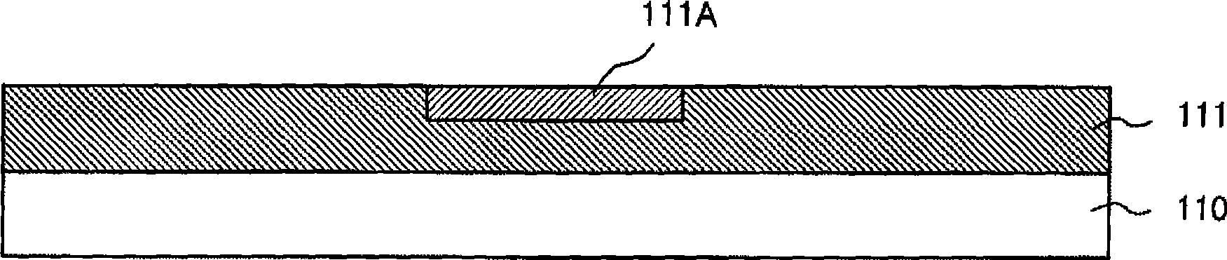
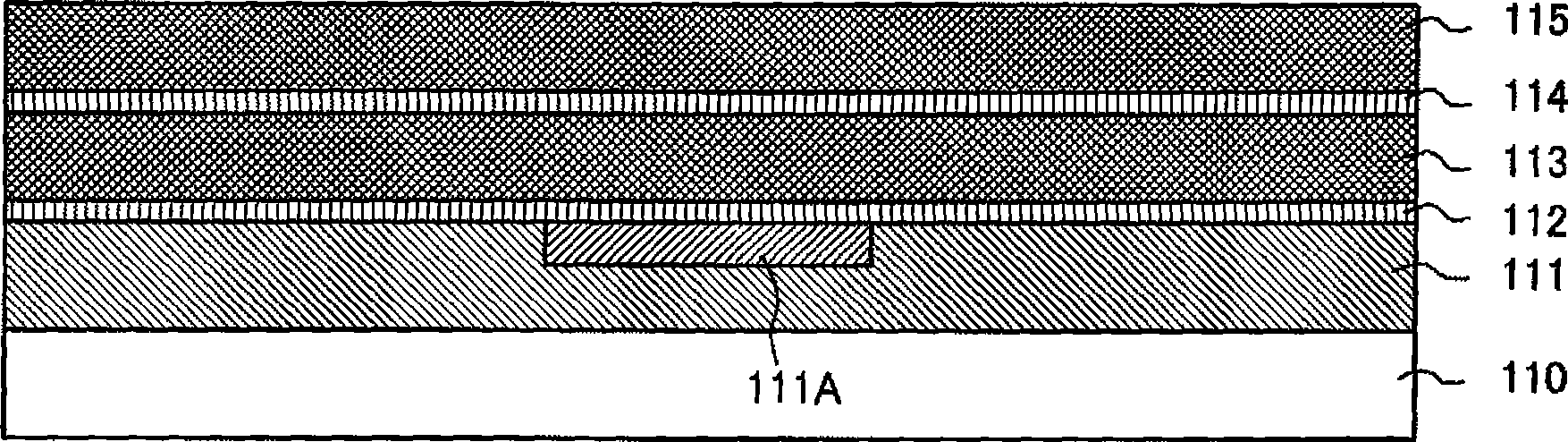
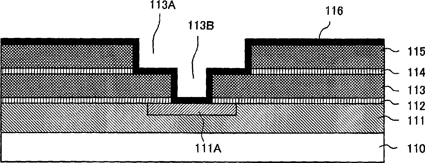
[0064] Figure 1A It is a cross-sectional view after forming a wiring pattern on a substrate. The silicon oxide film (SiO 2 On the film) 111, a wiring pattern 111A formed of a low-resistance metal such as copper (Cu) is embedded. Figure 1B is a cross-sectional view of a substrate after forming an interlayer insulating film on a wiring pattern. exist Figure 1B process, the SiO 2 On the film 111 are formed a low dielectric constant interlayer insulating film 113 , an etch stop film 114 such as a SiN film, and a low dielectric constant interlayer insulating film 115 via an etching stopper film 112 such as a silicon nitride film (SiN film).
[0065] For the interlayer insulating films 113, 115, for e...
specific example 1
[0095] 10 and 11 show the results of analysis in the depth direction by SIMS (Secondary Ion Mass Spectrometry: Secondary Ion Mass Spectrometry) when Cu is formed on TaN formed on a silicon thermal oxide film by applying an RF bias. The horizontal axis represents the depth from the surface, and the vertical axis represents ion intensity (Ion Intensity) (cps). Fig. 10 is the analysis result before annealing, and Fig. 11 is the depth direction analysis result after annealing the substrate at 500° C. for 1 hour. In Figure 10 and Figure 11, Cu is the atomic concentration (Cu Concentration) (atm / cm 3 ), whose scale is represented by the vertical axis on the right. The scale of the ion concentration (Ion Intensity) of other atoms is given by the vertical axis on the left.
[0096] In the figure, the thick solid line is the concentration of Cu, the white triangle is the concentration of Ta, the white square is the concentration of N, and the white circle is the concentration of Si. ...
specific example 2
[0103] 14 and 15 are diagrams showing SIMS analysis results in the case where Cu is formed on TaN formed on a fluorocarbon film by applying an RF bias. Fig. 14 shows the results before annealing, and Fig. 15 shows the analysis results after annealing at 200°C. In the figure, the thick solid line is the concentration of F, the dotted line is the concentration of C, the white circle is the concentration of Cu, the white triangle is the concentration of Ta, and the white square is the concentration of N. Concentration of F and C (F, C Concentration) (atm / cm 3 ) is represented by the scale on the right, and the intensity (Ion Intensity) (cps) of other atoms is represented by the scale on the left.
[0104] As shown in FIG. 14, F, C, and Ta diffused into Cu, but Cu did not diffuse into TaN before and after annealing. After annealing, Ta diffused into Cu.
[0105] 16 and 17 show SIMS analysis results in the case where Cu is formed on TaN formed on a fluorocarbon film without appl...
PUM
 Abstract
Description
Claims
Application Information
 - Generate Ideas
- Intellectual Property
- Life Sciences
- Materials
- Tech Scout
- Unparalleled Data Quality
- Higher Quality Content
- 60% Fewer Hallucinations
Browse by: Latest US Patents, China's latest patents, Technical Efficacy Thesaurus, Application Domain, Technology Topic, Popular Technical Reports.
© 2025 PatSnap. All rights reserved.Legal|Privacy policy|Modern Slavery Act Transparency Statement|Sitemap|About US| Contact US: help@patsnap.com