Touch control panel and touch control type LCD device
A liquid crystal display and touch panel technology, applied in static indicators, instruments, electrical digital data processing, etc., can solve problems such as maintenance difficulties, polarizer damage, scrapped display panels, etc., and achieve better fixability and flatness. Reduce the effect of using
- Summary
- Abstract
- Description
- Claims
- Application Information
AI Technical Summary
Problems solved by technology
Method used
Image
Examples
no. 1 example
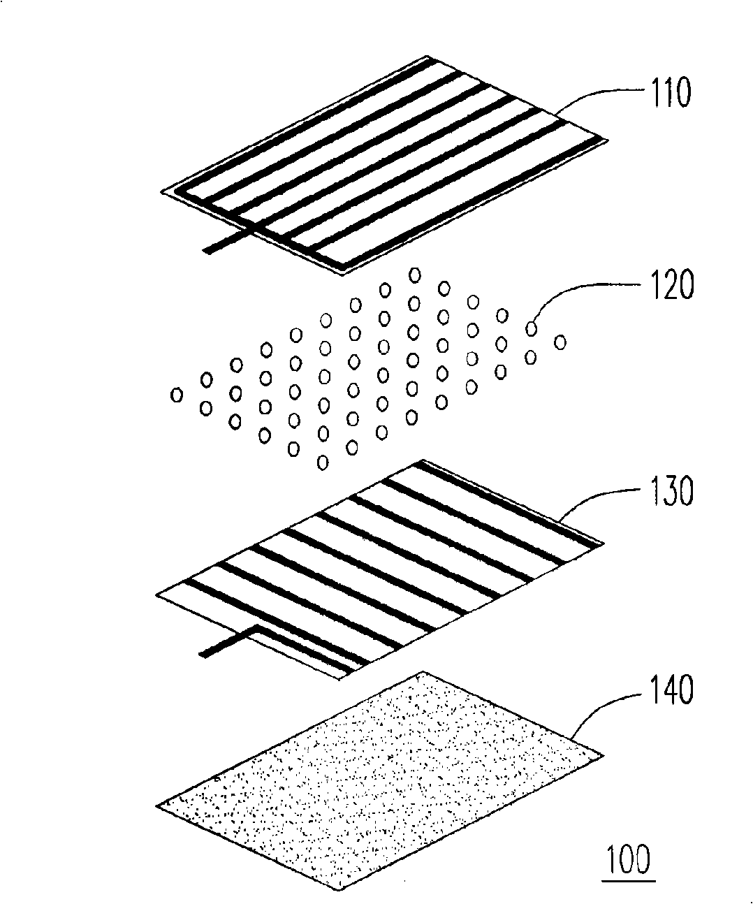
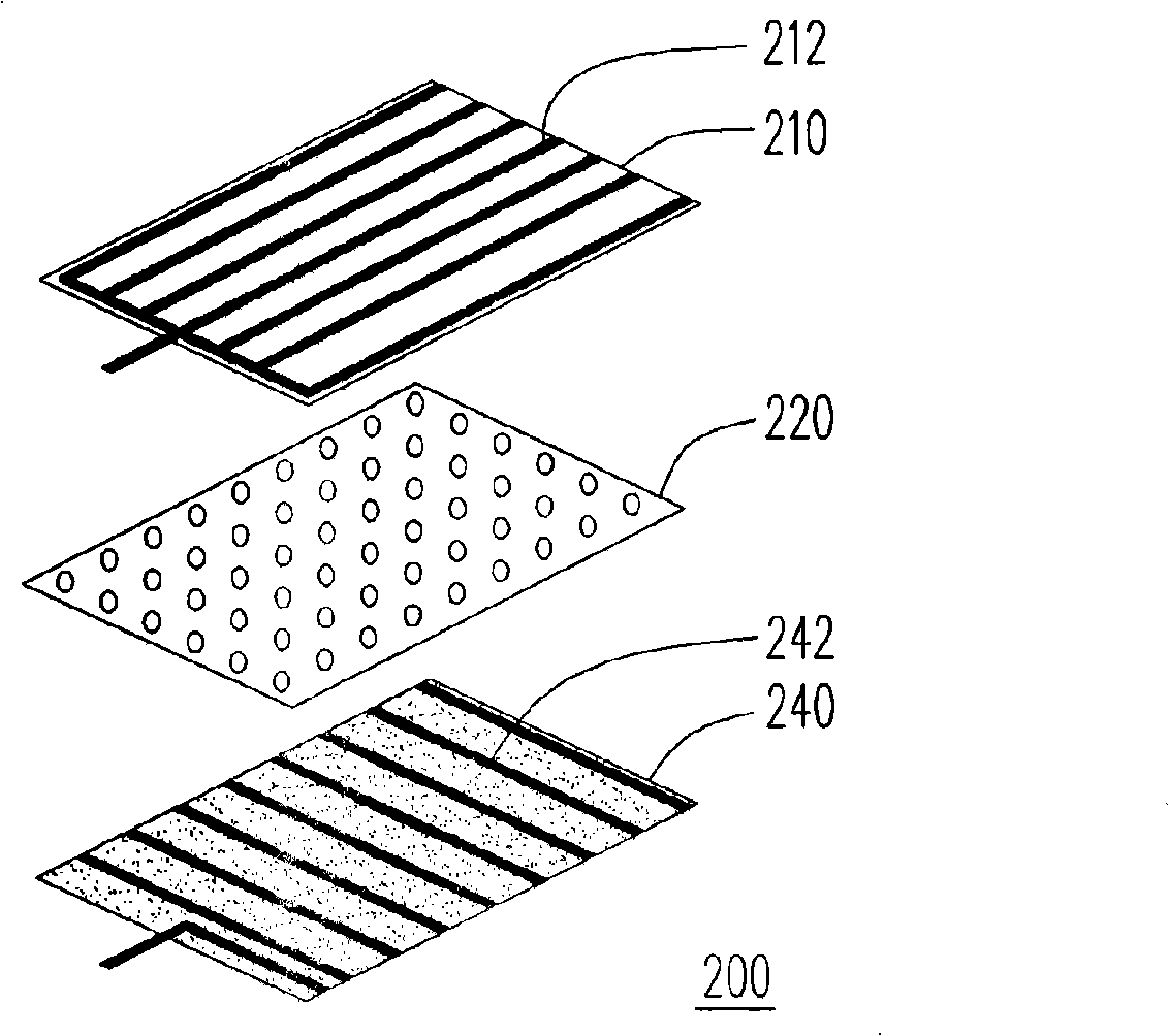
[0037] figure 2 It is a structure diagram of a resistive touch panel according to the first embodiment of the present invention. The touch panel 200 includes a contact layer 210 , an intermediate layer 220 and a polarizer 240 . The intermediate layer 220 is disposed between the contact layer 210 and the polarizer 240 for separating the contact layer 210 and the polarizer 240 . The contact layer 210 can be formed of PET film, glass or polymer film, and serves as an area where the user contacts with the touch panel. The middle layer 220 can be formed by supporting particles, and is used to separate the polarizer 240 from the contact layer 210 when the contact layer 210 is not stressed. The polarizer 240 has a polarizing function (limiting the angle through which light passes) and an electrical signal transmission function required by the touch panel.
[0038] The polarizer 240 has a plurality of first electrodes 242, and the contact layer 210 has a plurality of second electro...
no. 2 example
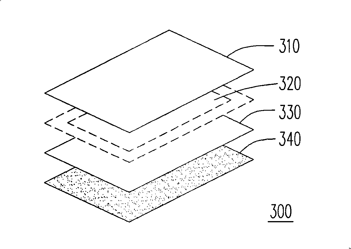
[0040] The above-mentioned technical means of the first embodiment can also be applied to capacitive touch panels, image 3 It is a structural diagram of a capacitive touch panel according to a second embodiment of the present invention. The touch panel 300 includes a protective layer 310, an electrode image layer 320, a conductive layer 330, and a polarizer 340, wherein the conductive layer 330 is disposed on the polarizer 340, and can be directly formed on the surface of the polarizer 340 by using indium tin oxide, so that It has electromagnetic shielding effect. The electrode image layer 320 is arranged between the protective layer 310 and the conductive layer 330, the upper and lower surfaces of the electrode image layer 320 respectively have a plurality of first electrodes and second electrodes to form the required electrode image, while the protective layer 310 It is arranged on the electrode image layer 320 to protect the electrode image layer 320 .
[0041] In anothe...
no. 3 example
[0043] Figure 4 It is a structural diagram of a touch-sensitive liquid crystal display according to a third embodiment of the present invention. This embodiment further illustrates the structural relationship between the resistive touch panel and the liquid crystal display panel. The liquid crystal display 400 includes a lower polarizer 420, a liquid crystal display unit 410, an upper polarizer 430, a contact layer 210, and an intermediate layer 220, wherein the upper polarizer 430, the contact layer 210 and the intermediate layer 220 form a touch panel, and its structure description please refer to figure 2 , no longer repeat. In this example, the figure 2 The illustrated polarizer 240 is directly applied in the liquid crystal display 400 as the upper polarizer 430 .
[0044] The liquid crystal display unit 410 includes at least a first substrate and a second substrate, and the upper polarizer 430 is located on the surface of the first substrate, and the lower polarizer...
PUM
 Abstract
Description
Claims
Application Information
 - R&D
- Intellectual Property
- Life Sciences
- Materials
- Tech Scout
- Unparalleled Data Quality
- Higher Quality Content
- 60% Fewer Hallucinations
Browse by: Latest US Patents, China's latest patents, Technical Efficacy Thesaurus, Application Domain, Technology Topic, Popular Technical Reports.
© 2025 PatSnap. All rights reserved.Legal|Privacy policy|Modern Slavery Act Transparency Statement|Sitemap|About US| Contact US: help@patsnap.com


