Electronic component comprising a p-doped organic semiconductor

A technology of organic semiconductors and electronic components, applied in the field of p-doped organic semiconductor materials, can solve problems such as toxicity

Active Publication Date: 2009-04-08
COMMISSARIAT A LENERGIE ATOMIQUE ET AUX ENERGIES ALTERNATIVES
View PDF10 Cites 5 Cited by
  • Summary
  • Abstract
  • Description
  • Claims
  • Application Information

AI Technical Summary

Problems solved by technology

Suitable p-dopants are usually organic dopants such as F4-TCNQ; these organic p-dopants are usually toxic

Method used


Image

  • Electronic component comprising a p-doped organic semiconductor

Examples


Embodiment Construction

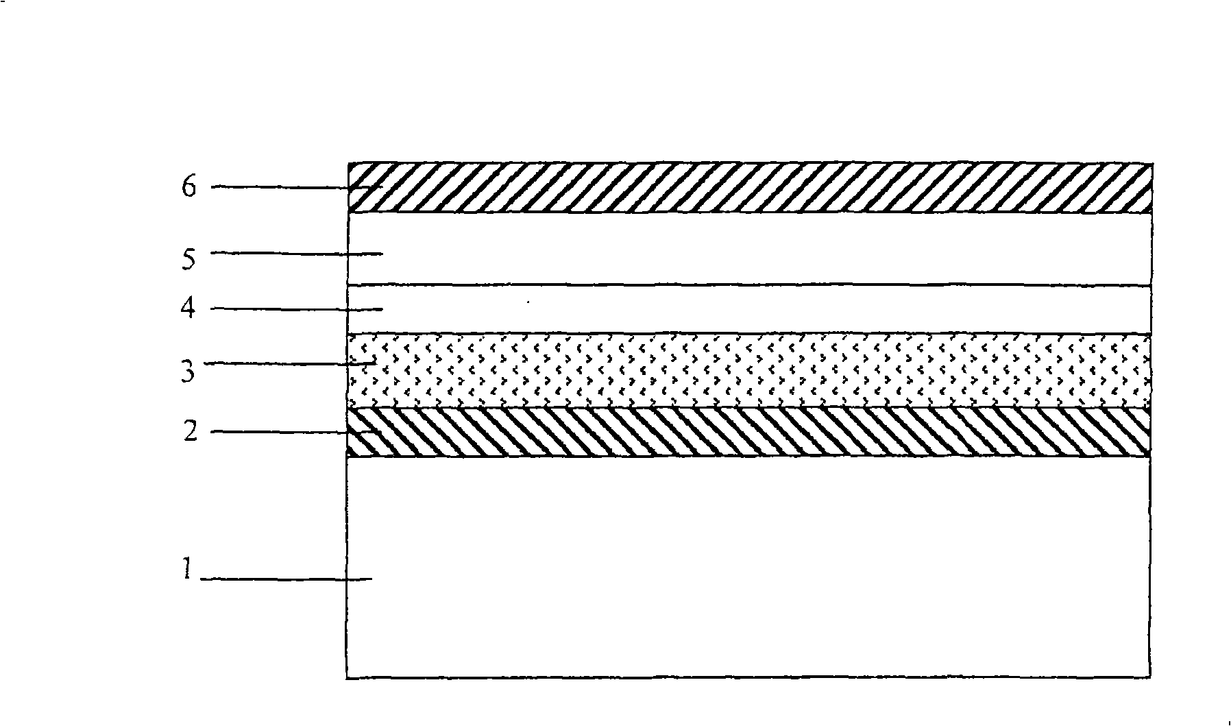
[0021] refer to figure 1 , the anode 2 is deposited on the insulating substrate 1 . The anode is made, for example, of ITO with a work function equal to 4.7 eV; the deposition is carried out in a conventional manner, eg cathode sputtering in vacuum.

[0022] A layer 3 of p-doped organic semiconductor material designed for hole transport purposes is subsequently deposited. The deposition is carried out by co-evaporation of the organic semiconducting material and a p-dopant in vacuum, where the p-dopant is an inorganic chemical element having an ionization potential higher than or equal to 4.7 eV; for example using cobalt or nickel; thus, with Unlike the p-doping described in documents EP0948063 and US4481132, the product co-deposited with the semiconductor is not an inorganic chemical salt element or a Lewis acid (Lewis acid); therefore, the degree of oxidation of the co-deposited element here is equal to zero, however when using a salt or a Lewis acid It is usually higher th...


PUM


Abstract

The invention relates to an electronic component comprising a layer of an organic semiconductor material in which a dopant is dispersed, the energetic difference between the output energy of the dopant and the HOMO level of the organic semiconductor material being lower than 0.5eV. The dopant is an atomic element having an evaporation temperature lower than 13000C, at a pressure of 10<-8> Torr. The invention eliminates any toxicity problems related to usual organic acceptor dopants, and especially applies to organic electroluminescent diodes.

Description

technical field [0001] The present invention relates to p-doped organic semiconducting materials having a base formed especially by small molecules (as opposed to polymers), and the applications of these doped semiconductors, in particular light-emitting diodes, organic transistors or any other electronic element. A p-dopant is an electron acceptor dopant; thus it is generally oxidizing to the material it is doped with. Background technique [0002] The fabrication of transistors or diodes from organic semiconductors with a matrix formed of small molecules usually requires a vacuum deposition step on a substrate, which is usually previously provided with one or more electrodes called bottom electrodes; In , semiconductor molecules are evaporated in a vacuum chamber so that they recondense on the substrate to form a deposited layer; one or more electrodes, called top electrodes, are usually subsequently deposited on the organic layer. [0003] Document US6525465 relates to ...

Claims


Application Information

Patent Timeline
Patent Type & Authority Applications(China)
IPC IPC(8): H01L51/52
CPCH01L51/002H01L51/5088H01L51/105H10K71/30H10K10/84H10K50/17H10K2101/30Y10S428/917
Inventor 穆罕麦德·本卡利法戴维·沃弗里
Owner COMMISSARIAT A LENERGIE ATOMIQUE ET AUX ENERGIES ALTERNATIVES
Why Eureka
Try Eureka