
Circuit board, electronic circuit device, and display

A circuit substrate and electronic circuit technology, applied in the direction of circuits, printed circuits, printed circuits, etc., can solve the problems of setting wiring, not being able to set wiring at high density, and not being able to set wiring at high density, so as to achieve the balance of suppressing edge short circuit and pressure sex good effect

Active Publication Date: 2009-04-01
SHARP KK
View PDF3 Cites 3 Cited by
  • Summary
  • Abstract
  • Description
  • Claims
  • Application Information

AI Technical Summary

Problems solved by technology

However, with this technology, only one wiring can be placed on the back of the area where the IC is mounted, so it is not possible to install wiring at a high density
[0008] In addition, the inventions described in Patent Document 2 and Patent Document 3 are not techniques for suppressing edge short circuits. In addition, the invention described in Patent Document 3 can only provide one wiring on the back surface of the IC mounting part, and Patent Document 2 The same is true for the invention described in , since no wiring is provided on the back side of the mounting part, it is not possible to provide high-density wiring
[0009] Therefore, there is still room for improvement in conventional circuit boards in terms of both high-density wiring and suppression of edge short circuits.

Method used


Image

  • Circuit board, electronic circuit device, and display
  • Circuit board, electronic circuit device, and display
  • Circuit board, electronic circuit device, and display

Examples


Embodiment approach 1

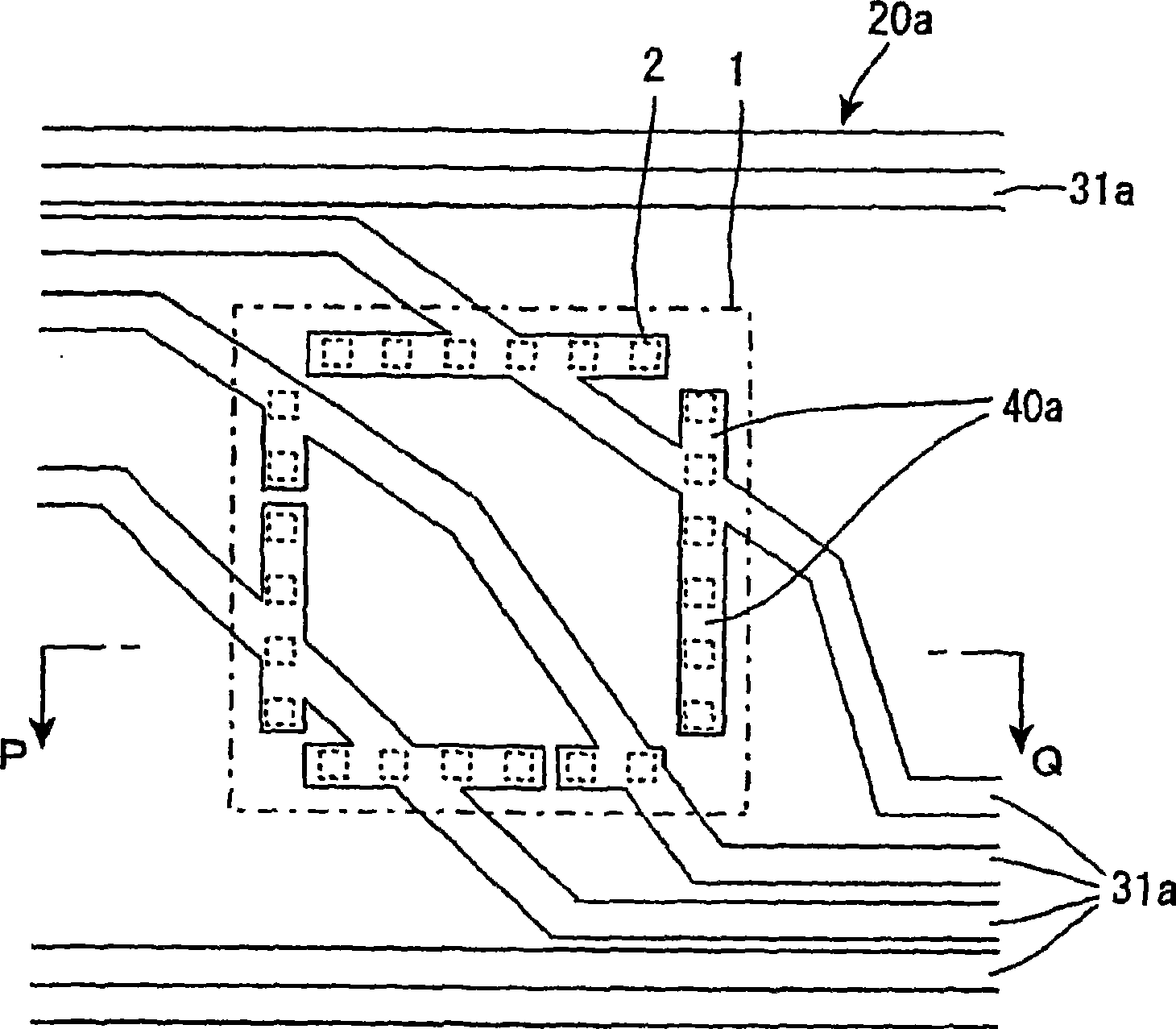
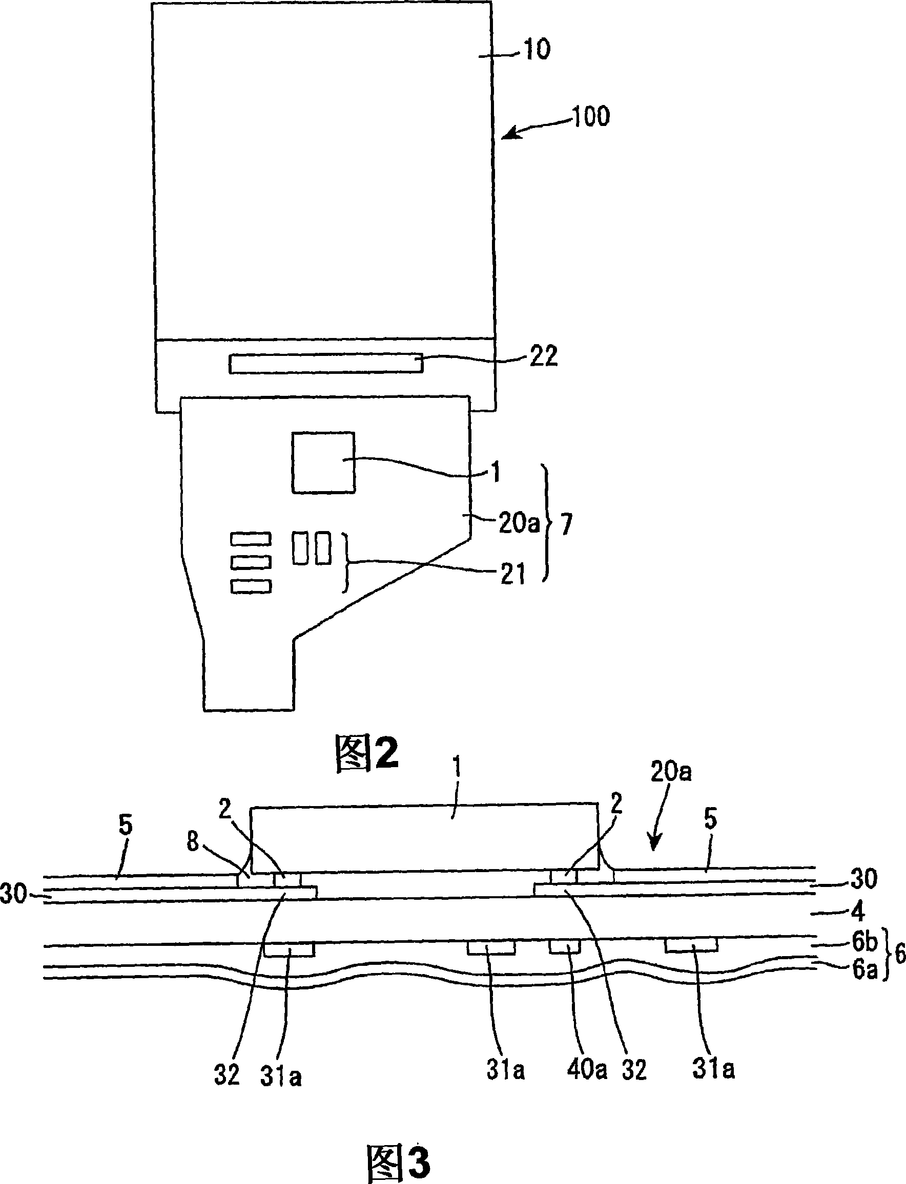
[0106] A liquid crystal display device according to Embodiment 1 of the present invention will be described. FIG. 2 is a schematic plan view of the liquid crystal display device of the present embodiment.

[0107] The liquid crystal display device 100 includes a liquid crystal display panel 10 and an electronic circuit device 7 connected to an end of the liquid crystal display panel 10 .

[0108] The liquid crystal display panel 10 includes an element substrate on which switching elements are formed, an opposing substrate disposed opposite to the element substrate, and a liquid crystal layer interposed between the two substrates. The counter substrate includes a common electrode and a color filter layer provided on the substrate substantially over the entire surface of the display region. The liquid crystal layer is composed of a nematic liquid crystal material with electro-optical properties.

[0109] The element substrate includes a plurality of gate wirings extending para...

Embodiment approach 2

[0156] Next, a liquid crystal display device according to Embodiment 2 of the present invention will be described. The liquid crystal display device of Embodiment 2 differs from Embodiment 1 only in the form of the second wiring and the wiring portion, and therefore descriptions of the contents that overlap in Embodiments 1 and 2 are omitted.

[0157] Image 6 It is a plan schematic view showing the structure of the IC chip mounting region and its vicinity on the second main surface (rear surface) side of the electronic circuit device according to the second embodiment. Among them, in Image 6 In , the dotted line and the dashed-dotted line represent the bumps and the IC chip disposed on the first main surface (surface), respectively.

[0158] In the liquid crystal display device (circuit board 20 b ) of this embodiment, the second wiring 31 b and the wiring portion 40 b are not connected to each other. That is, the wiring part 31b is a dummy wiring electrically insulated f...

Embodiment approach 3

[0163] Next, a liquid crystal display device according to Embodiment 3 of the present invention will be described. The liquid crystal display device of Embodiment 3 differs from Embodiment 1 only in the form of the second wiring and the wiring portion, and therefore descriptions of the contents that overlap in Embodiments 1 and 3 are omitted.

[0164] 7 is a schematic plan view showing the structure of an IC chip mounting region and its vicinity on the second main surface (rear surface) side of the electronic circuit device according to Embodiment 3. FIG. Here, in FIG. 7 , dotted lines and dashed-dotted lines represent the bumps and the IC chip disposed on the first main surface (surface), respectively.

[0165] The liquid crystal display device (circuit board 20c) of this embodiment includes the second wiring 31c and the wiring portion 40c having a gap. That is, gaps are provided between the respective wiring portions 40c. In addition, the interval Dc between the respective...


PUM


Abstract

A circuit board, an electronic circuit device, and a display device, in which generation of an edge short-circuit is prevented, includes wirings that are arranged much more densely. A circuit board includes a substrate having a first main surface on which a semiconductor integrated circuit is mounted and a second main surface; a plurality of first wirings including a bump connecting terminal on the first main surface; and a plurality of second wirings on the second main surface, wherein the plurality of the second wirings are arranged independently from each other and overlap with a region where the semiconductor integrated circuit is mounted, and the circuit board includes a wiring portion on the second main surface in a region overlapping with a region where the bump connecting terminal is arranged.

Description

technical field [0001] The present invention relates to a circuit substrate, an electronic circuit device and a display device. More specifically, it relates to a circuit board suitable for face-down mounting of semiconductor integrated circuits, and an electronic circuit device and a display device including the circuit board. Background technique [0002] Due to the high functionality and miniaturization of electronic equipment represented by mobile phones, components mounted on substrates are becoming denser. In this way, the wiring formation of the circuit board is also progressing from single-sided formation to double-sided formation and multi-layer formation, and higher density of wiring is also required. [0003] Here, a method of mounting a semiconductor integrated circuit (hereinafter also referred to as an "IC chip") on a circuit board on which wiring is formed at a high density on both sides, especially on the back side, will be described. [0004] Figure 13 It...

Claims


Application Information

Patent Timeline
Patent Type & Authority Applications(China)
IPC IPC(8): H05K3/46H01L21/60
CPCH01L2224/83851H01L24/83H01L2224/29344H01L2924/01004H05K1/189H05K2201/09781H01L2224/16H01L2924/01322H01L2224/29355H05K2201/10674H01L23/49838H01L2224/81191H01L2224/32225H01L2224/16238H05K2201/2009H01L2224/2929H01L2224/73204H01L2924/01079G02F1/13452H01L2924/14H01L2924/01078H01L24/16H01L2224/16225H01L24/31H01L2924/12044H05K1/0271H01L2924/00011H01L2924/00014H01L2924/12042H01L2924/00012H01L2924/0665H01L2924/00H01L2224/0401
Inventor 中滨裕喜村冈盛司
Owner SHARP KK
Learn More