Large power LED encapsulation method
A LED packaging and high-power technology, which is applied in the direction of electrical components, circuits, semiconductor devices, etc., can solve the problems of low production efficiency and poor heat dissipation effect, and achieve the effects of improving production efficiency, reducing filling of silicone resin, and realizing mechanized operation
- Summary
- Abstract
- Description
- Claims
- Application Information
AI Technical Summary
Problems solved by technology
Method used
Image
Examples
Embodiment Construction
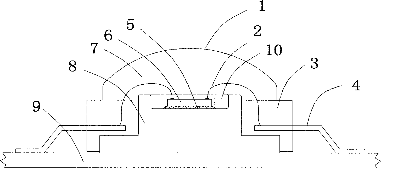
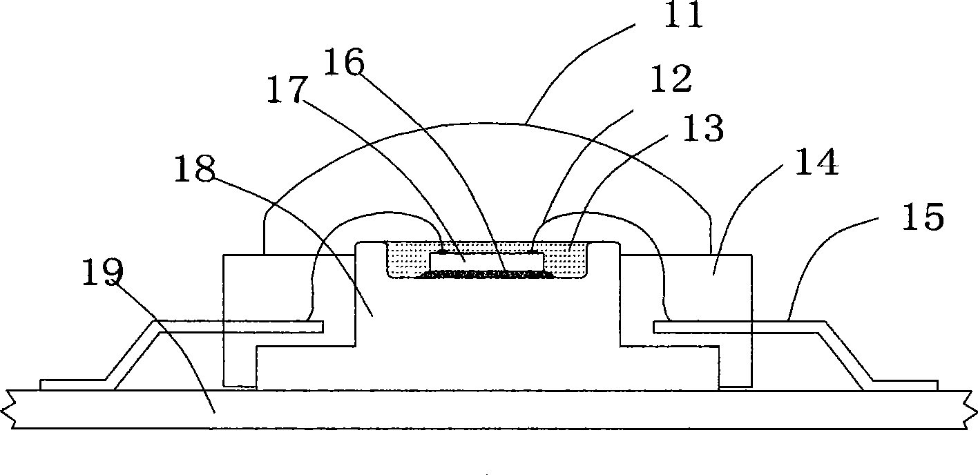
[0015] refer to figure 2 , which shows a schematic cross-sectional view of a finished LED structure in a high-power packaging method according to the present invention. The structure of the finished product includes lens 11 , inner lead 12 , fluorescent powder 13 , insulating molding material 14 , outer lead (ie, mounting pin) 15 , soldering metal 16 , LED chip 17 , heat conduction column 18 , and heat dissipation substrate 19 .
[0016] In the high-power LED packaging method of the present invention, small granulated solder metal 16 is first placed on the fixed chip of the heat conduction column 18, and then enters the reflow soldering machine for welding, and the LED chip 17 is firmly welded in the middle of the heat conduction column 18; Use a gold wire welding machine to connect the LED chip 17 with the inner lead 12 and the outer lead 15, put phosphor powder 13 on the LED chip 17 and then dry it to form a semi-finished product; prepare for potting the lens; then, after h...
PUM
 Abstract
Description
Claims
Application Information
 - R&D Engineer
- R&D Manager
- IP Professional
- Industry Leading Data Capabilities
- Powerful AI technology
- Patent DNA Extraction
Browse by: Latest US Patents, China's latest patents, Technical Efficacy Thesaurus, Application Domain, Technology Topic, Popular Technical Reports.
© 2024 PatSnap. All rights reserved.Legal|Privacy policy|Modern Slavery Act Transparency Statement|Sitemap|About US| Contact US: help@patsnap.com


