Cdm ESD protection for integrated circuits

A technology of circuit and clamping circuit, applied in the field of electrostatic discharge protection circuit system, can solve problems such as threats

Inactive Publication Date: 2009-04-01
SARNOFF CORP +1
View PDF1 Cites 8 Cited by
  • Summary
  • Abstract
  • Description
  • Claims
  • Application Information

AI Technical Summary

Problems solved by technology

Therefore, these isolation wells, such as P-well isolation region 106, can pose a threat to IC 100 during CDM stress

Method used


Image

  • Cdm ESD protection for integrated circuits
  • Cdm ESD protection for integrated circuits
  • Cdm ESD protection for integrated circuits

Examples


Embodiment Construction

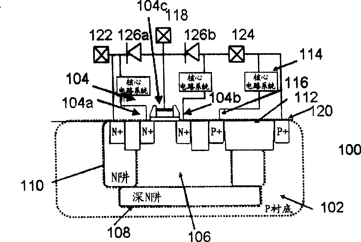
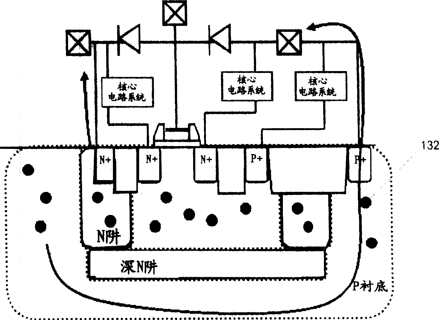
[0023] The present invention relates to a technique to increase the CDM performance of an IC by connecting an additional ESD clamp circuit to the isolation well (or junction). Figure 2A shows a cross-sectional view of an integrated circuit IC 200 for CDM ESD protection according to one embodiment of the present invention. IC 200 shows a cross-sectional view of transistor 104 formed in isolated P-well region 106 , deep N-well 108 and N-well 110 form a ring structure around the isolation region to isolate / separate P-well region 106 from P-substrate 104 . Additionally, an additional ESD clamp circuit 202 is coupled to the isolated P-well 106, as shown in FIG. 2A. Specifically, ESD clamp circuit 202 is placed between isolated P-well 106 and the reference node. Selection of the reference node depends on normal operating requirements such as noise, cross-coupling, and other ESD factors. Preferably for ESD and in this example of FIG. 2A , the terminal to the isolated well 106 is co...


PUM


Abstract

The present invention provides a charged-device model (CDM) electrostatic discharge (ESD) protection circuit for an integrated circuit (IC). The ESD protection circuit comprises a substrate of first conductivity type; a MOS component of second conductivity type formed on a first well on the substrate, and coupled to a pad; an isolating well / region having the second conductivity type being formed between the first well and the substrate to separate the first well and the substrate. Additionally, the circuit comprises an ESD clamp coupled to the isolated well / region. Under normal power operation, the ESD clamp is open. During a CDM ESD event, the CDM charges accumulated in the substrate and the MOS component are removed by the ESD clamp to prevent damage to the IC.

Description

technical field [0001] The present invention relates generally to the field of electrostatic discharge (ESD) protection circuitry, and more particularly to improvements to the Charged Device Model (CDM) stress profile in protection circuitry for integrated circuits (ICs). Background technique [0002] Integrated circuits (ICs) and other semiconductor devices are very sensitive to the high voltages that may be generated in connection with ESD events. Thus, electrostatic discharge (ESD) protection circuitry is necessary for integrated circuits. ESD events are usually produced by the discharge of a high voltage potential (typically several thousand volts) and result in a pulse of high current (several amperes) of short duration (typically 100 nanoseconds). An ESD event can occur within an IC, for example, by a person coming into contact with a lead of the IC or by a live machine being discharged in another lead of the IC. During installation of the integrated circuit into a p...

Claims


Application Information

Patent Timeline
Patent Type & Authority Applications(China)
IPC IPC(8): H01L27/02H01L27/04H02H9/00
CPCH01L2924/0002H01L27/0251H01L2924/00
Inventor B·V·坎普B·索尔格洛斯
Owner SARNOFF CORP
Why Eureka
Try Eureka