Bendable low radiation coated glass
A technology of low-emissivity coating and coated glass, applied in the field of coated glass, can solve the problems that the film layer cannot withstand high temperature for a long time and the solar transmittance is reduced, and achieves the effect of clear appearance, saving heating costs, and saving cooling costs.
- Summary
- Abstract
- Description
- Claims
- Application Information
AI Technical Summary
Problems solved by technology
Method used
Image
Examples
Embodiment 1
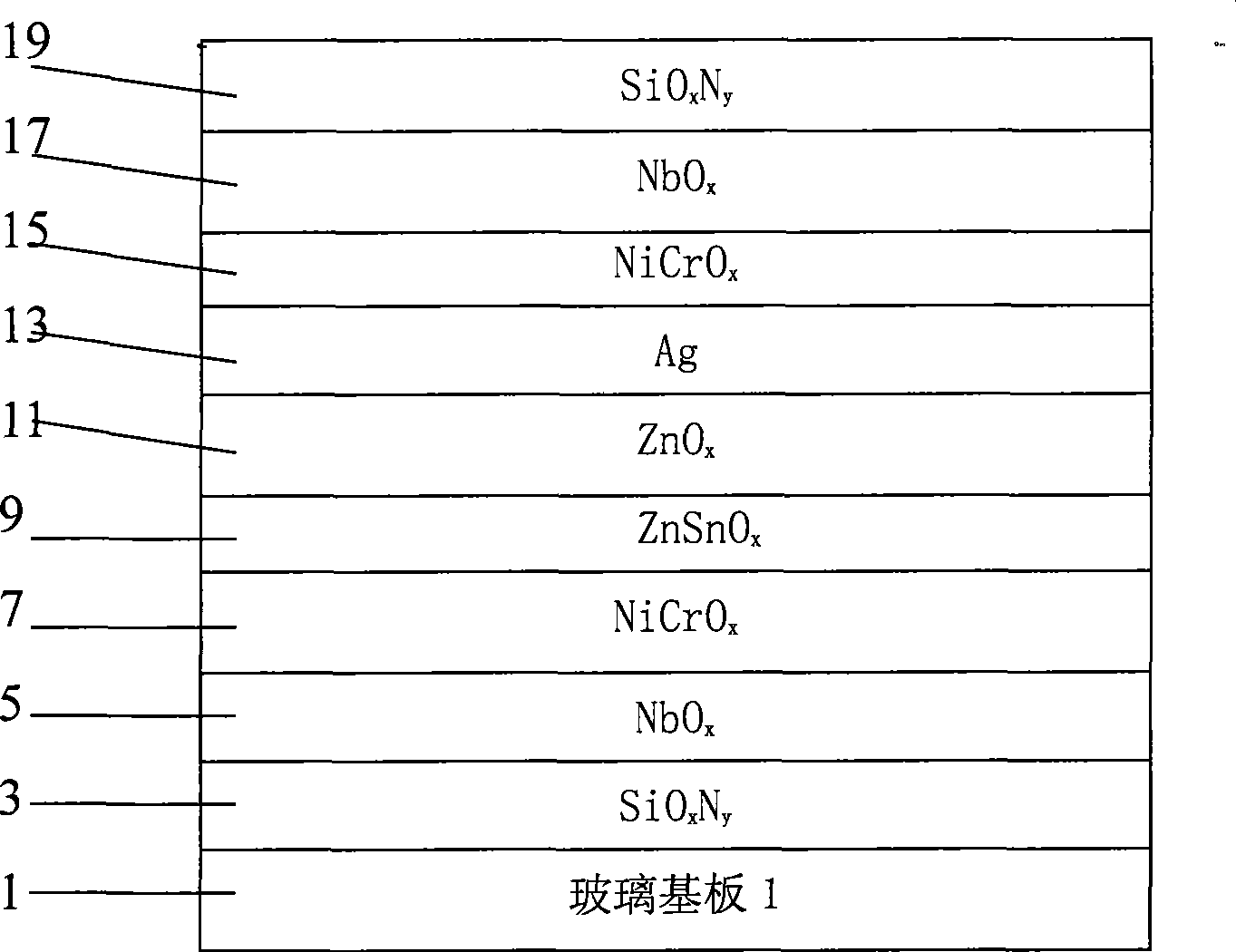
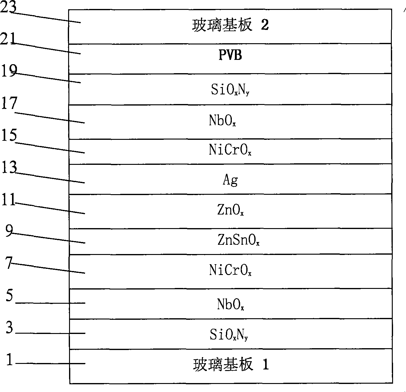
[0039] The first dielectric layer is first plated on the clean green float glass with a thickness of 1.8mm (produced by Fuqing Factory of Fuyao Glass Group Float Division) after washing, polishing, and drying, that is, in order Coated with SiO x N y / NbO x / NiCrO x / ZnSnO x / ZnO x film layer, which is coated with SiO x N y The film layer uses a rotating target, plated with NbO x , NiCrO x , ZnSnO x The target used for the film layer is a planar target, ZnO x The film layer uses a rotating target; where,
[0040] SiO x N y In the film layer, x=0.3, y=1.5, and the film thickness is 40nm;
[0041] NbO x In the film layer, x=1.7 and the thickness is 12nm;
[0042] NiCrO x In the film layer, x=0.3 and the thickness is 15nm;
[0043] ZnSnO x In the film layer, x=1.8 and the thickness is 12nm;
[0044] ZnO x In the film layer, x=0.8, and the thickness is 8nm.
[0045] Secondly, a low-emissivity film layer, ie, an Ag layer, is coated. The target material used is a...
Embodiment 2
[0055] On the clean green float glass with a thickness of 2.1mm after washing, polishing and drying (produced by Fuqing Factory of Fuyao Glass Group Float Division), SiO2 is plated in sequence. x N y / SnO x / NiCrO x / SnO x / Ag / NiCrO x / SnO x / SiO x N y film layer, of which:
[0056] SiO x N y In the film layer, x=1.5, y=0.33, and the film thickness is 35nm;
[0057] SnO x In the film layer, x=1.5 and the thickness is 15nm;
[0058] NiCrO x In the film layer, x=0.3, and the thickness is 23nm;
[0059] SnO x In the film layer, x=1.5, and the thickness is 12nm.
[0060] Secondly, a low-radiation film layer, ie, an Ag layer, is plated on, and the thickness of the film layer is 15nm.
[0061] Then the second dielectric layer is plated, and NiCrO is plated in sequence x / SnO x layer;
[0062] NiCrO x In the film layer, x=0.3 and the thickness is 20nm;
[0063] SnO x In the film layer, x=1.6, and the thickness is 15nm.
[0064] Finally, a protective layer is pl...
PUM
| Property | Measurement | Unit |
|---|---|---|
| Thickness | aaaaa | aaaaa |
| Film thickness | aaaaa | aaaaa |
| Thickness | aaaaa | aaaaa |
Abstract
Description
Claims
Application Information
 - R&D
- Intellectual Property
- Life Sciences
- Materials
- Tech Scout
- Unparalleled Data Quality
- Higher Quality Content
- 60% Fewer Hallucinations
Browse by: Latest US Patents, China's latest patents, Technical Efficacy Thesaurus, Application Domain, Technology Topic, Popular Technical Reports.
© 2025 PatSnap. All rights reserved.Legal|Privacy policy|Modern Slavery Act Transparency Statement|Sitemap|About US| Contact US: help@patsnap.com


