Organic electroluminescent device
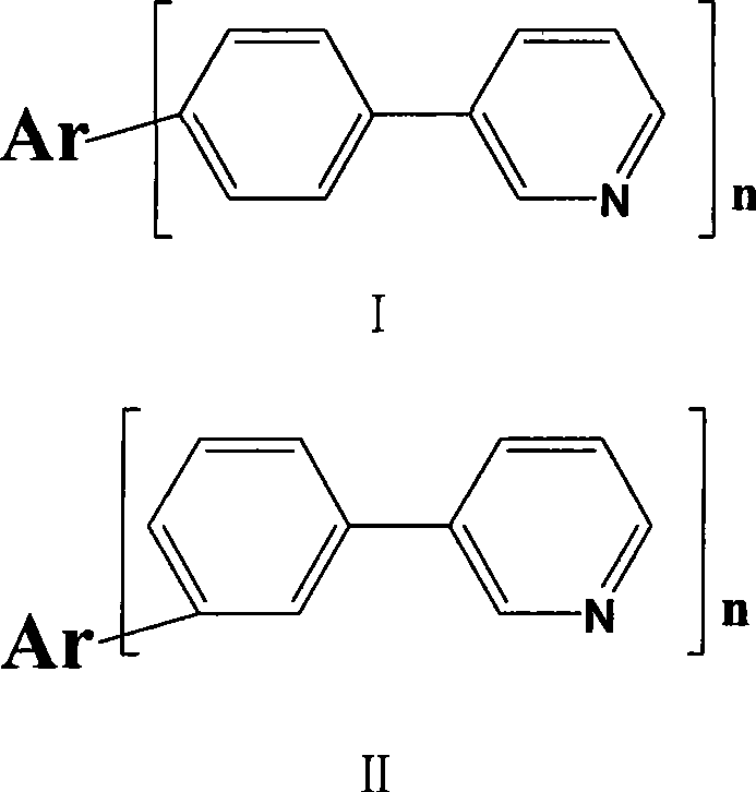
An electroluminescent device and electroluminescent technology, which is applied in the fields of electro-solid devices, electrical components, organic chemistry, etc., can solve the problems of increasing the complexity of the device manufacturing process, reducing the cost of OLEDs, disadvantages, etc., and enhancing the ability to provide electrons, Effects of high electron transport capability, high electron injection capability
- Summary
- Abstract
- Description
- Claims
- Application Information
AI Technical Summary
Problems solved by technology
Method used
Image
Examples
Embodiment 1
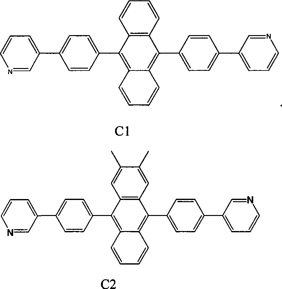
[0041] Device structure: ITO / NPB(40nm) / AND(30nm):7%TBPe / Compound C1(30nm) / LiF / Al
[0042] With the ITO conductive glass substrate etched with specific patterns as the substrate, the substrate is ultrasonically cleaned in deionized water containing cleaning solution. The temperature of the cleaning solution is about 60°C, and then the cleaned substrate is cleaned Dry it, put it into the evaporation chamber to evaporate the hole injection layer, the hole transport layer, the light emitting layer, the electron transport layer, the electron injection layer, and the cathode structure in sequence, and the chamber pressure during the evaporation process is lower than 5.0×10- 3Pa. In this embodiment, the organic layer is first vapor-deposited 40nm thick N, N'-bis-(1-naphthyl)-N, N'-diphenyl-1,1'-biphenyl-4,4'-diamine (NPB) as the empty Hole transport layer; 30nm thick 9,10-Di(naphth-2-yl)anthracene (ADN) and 2,5,8,11-Tetra-tert-butylperylene (TBPe) were evaporated by double source co...
Embodiment 2
[0044] Device structure: ITO / NPB(40nm) / AND(30nm):7%TBPe / PADN(20nm) / compound C5(10nm) / LiF / Al
[0045] With the ITO conductive glass substrate etched with specific patterns as the substrate, the substrate is ultrasonically cleaned in deionized water containing cleaning solution. The temperature of the cleaning solution is about 60°C, and then the cleaned substrate is cleaned Dry it, put it into the evaporation chamber to evaporate the hole injection layer, the hole transport layer, the light emitting layer, the electron transport layer, the electron injection layer, and the cathode structure in sequence, and the chamber pressure during the evaporation process is lower than 5.0×10- 3Pa. In this embodiment, the organic layer is first vapor-deposited 40nm thick N, N'-bis-(1-naphthyl)-N, N'-diphenyl-1,1'-biphenyl-4,4'-diamine (NPB) as the empty Hole transport layer; 30nm thick 9,10-Di(naphth-2-yl)anthracene (ADN) and 2,5,8,11-Tetra-tert-butylperylene (TBPe) were evaporated by doubl...
Embodiment 3
[0047] Device structure: ITO / NPB(40nm) / AND(30nm):7%TBPe / Compound C11(20nm) / Alq3(10nm) / LiF / Al
[0048] With the ITO conductive glass substrate etched with specific patterns as the substrate, the substrate is ultrasonically cleaned in deionized water containing cleaning solution. The temperature of the cleaning solution is about 60°C, and then the cleaned substrate is cleaned Dry it, put it into the evaporation chamber to evaporate the hole injection layer, the hole transport layer, the light emitting layer, the electron transport layer, the electron injection layer, and the cathode structure in sequence, and the chamber pressure during the evaporation process is lower than 5.0×10- 3Pa. In this embodiment, the organic layer is first vapor-deposited 40nm thick N, N'-bis-(1-naphthyl)-N, N'-diphenyl-1,1'-biphenyl-4,4'-diamine (NPB) as the empty Hole transport layer; 30nm thick 9,10-Di(naphth-2-yl)anthracene (ADN) and 2,5,8,11-Tetra-tert-butylperylene (TBPe) were evaporated by doub...
PUM
 Abstract
Description
Claims
Application Information
 - R&D
- Intellectual Property
- Life Sciences
- Materials
- Tech Scout
- Unparalleled Data Quality
- Higher Quality Content
- 60% Fewer Hallucinations
Browse by: Latest US Patents, China's latest patents, Technical Efficacy Thesaurus, Application Domain, Technology Topic, Popular Technical Reports.
© 2025 PatSnap. All rights reserved.Legal|Privacy policy|Modern Slavery Act Transparency Statement|Sitemap|About US| Contact US: help@patsnap.com


