FIFO burst buffer with large capacity based on SDRAM and data storage method
A technology of data storage and buffer, applied in the field of burst buffer, which can solve the problems of small FIFO burst buffer capacity, inability to complete read and write operations at the same time, and high price
- Summary
- Abstract
- Description
- Claims
- Application Information
AI Technical Summary
Problems solved by technology
Method used
Image
Examples
specific Embodiment approach 1
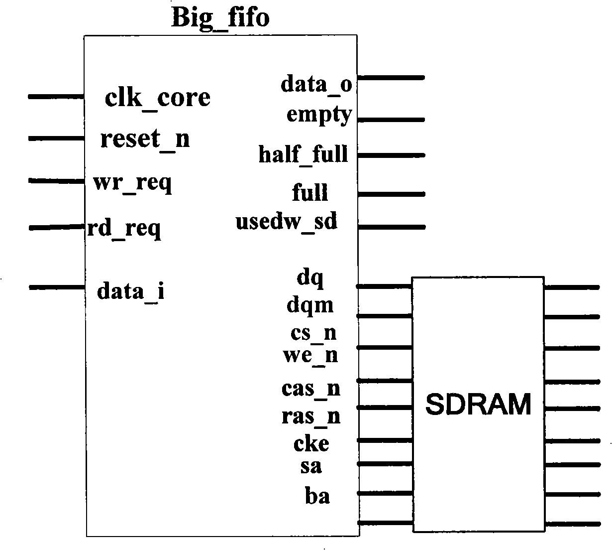
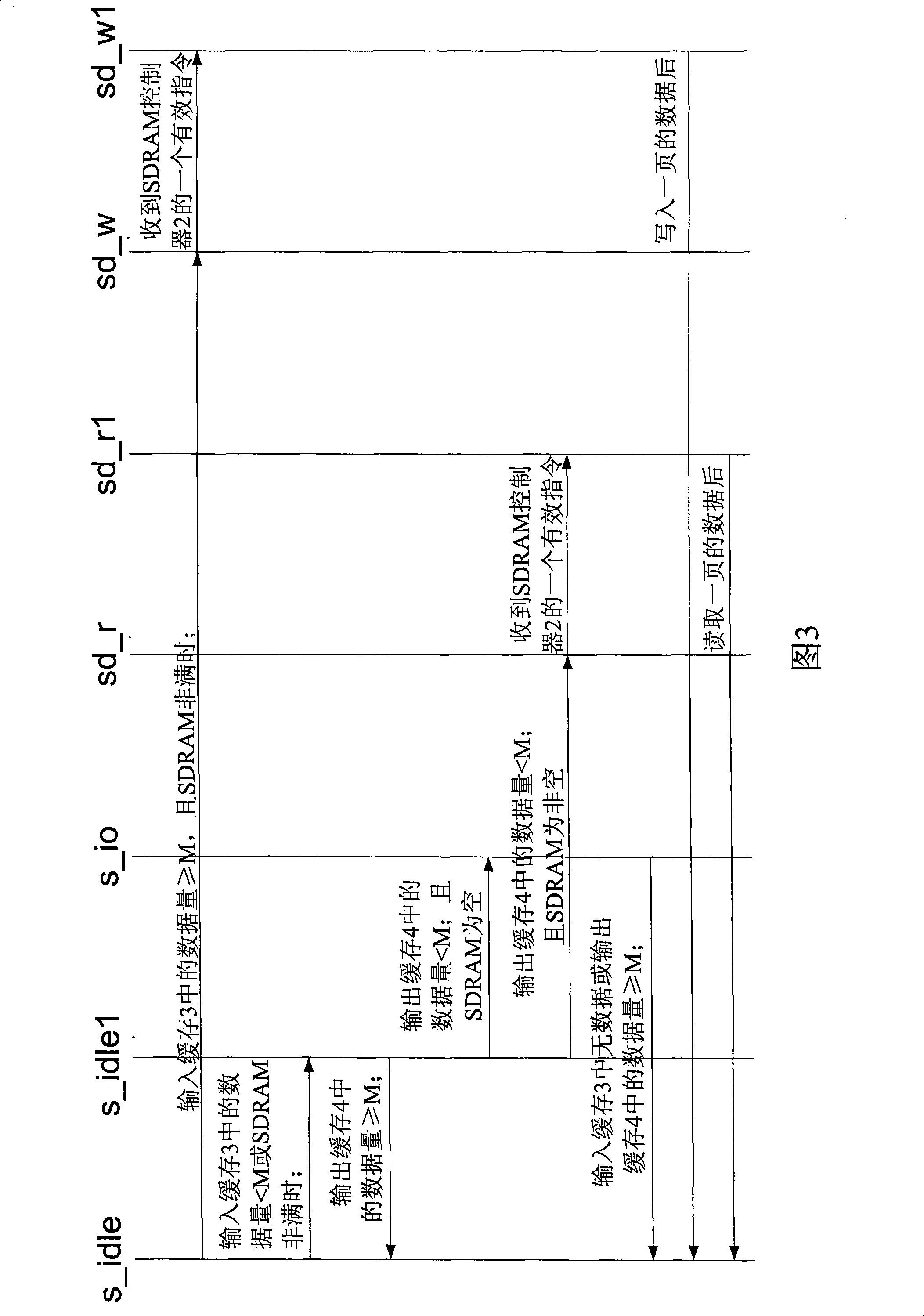
[0025] Specific implementation mode one: combine figure 1 Describe this embodiment mode, it is based on the large-capacity FIFO burst register master controller 1 of SDRAM, SDRAM controller 2, input buffer 3 and output buffer 4 to form; The data input end of input buffer 3 is the external data input end , the read control end of the input buffer 3 is connected to the input buffer control end of the main controller 1, and the SDRAM memory data output end of the input buffer 3 is connected to the data input end of the SDRAM controller 2; the data input end of the input buffer 3 is directly output Connect the data direct input end of the output buffer 4; the write control end of the output buffer 4 is connected to the output buffer control end of the main controller 1, and the SDRAM memory data input end of the output buffer 4 is connected to the data output end of the SDRAM controller 2 , the data output end of the output buffer 4 is an external data output end; the SDRAM read-...
specific Embodiment approach 2
[0026] Embodiment 2: This embodiment differs from Embodiment 1 in that the input buffer 3 and the output buffer 4 are two small-capacity FIFO memories. Other compositions and connection methods are the same as those in Embodiment 1.
specific Embodiment approach 3
[0027] Specific implementation mode three: combination figure 2 Describe this embodiment, the difference between this embodiment and specific embodiment one is that the whole system of this embodiment is implemented in FPGA, and the input buffer 3 and output buffer 4 used as data buffering all use the small-capacity FIFO module inside FPGA Realize, SDRAM controller 2 adopts the SDRAM memory inside FPGA, the SDRAM memory of DDR or DDRII series;
[0028] This implementation mode adopts the VHDL language to be written and applied on the Quartus II software. Before applying this system, the SDRAM to be used must be determined. According to the selected SDRAM data sheet, some important parameters, the bit width DSIZE of the data, and each BANK address row number ROWSIZE and column number COLSIZE, BANK number BANKSIZE, core clock rate clk_core, refresh command duration t RFC , precharge effective time tRP , the time interval t between column read and write commands and row effecti...
PUM
 Abstract
Description
Claims
Application Information
 - Generate Ideas
- Intellectual Property
- Life Sciences
- Materials
- Tech Scout
- Unparalleled Data Quality
- Higher Quality Content
- 60% Fewer Hallucinations
Browse by: Latest US Patents, China's latest patents, Technical Efficacy Thesaurus, Application Domain, Technology Topic, Popular Technical Reports.
© 2025 PatSnap. All rights reserved.Legal|Privacy policy|Modern Slavery Act Transparency Statement|Sitemap|About US| Contact US: help@patsnap.com


