Integrating analog to digital converter
An analog-to-digital converter and integration technology, applied in the field of ADC, can solve the problems affecting the output accuracy, etc., and achieve the effect of high sampling frequency, good resolution and low power consumption
- Summary
- Abstract
- Description
- Claims
- Application Information
AI Technical Summary
Problems solved by technology
Method used
Image

Examples
Embodiment Construction
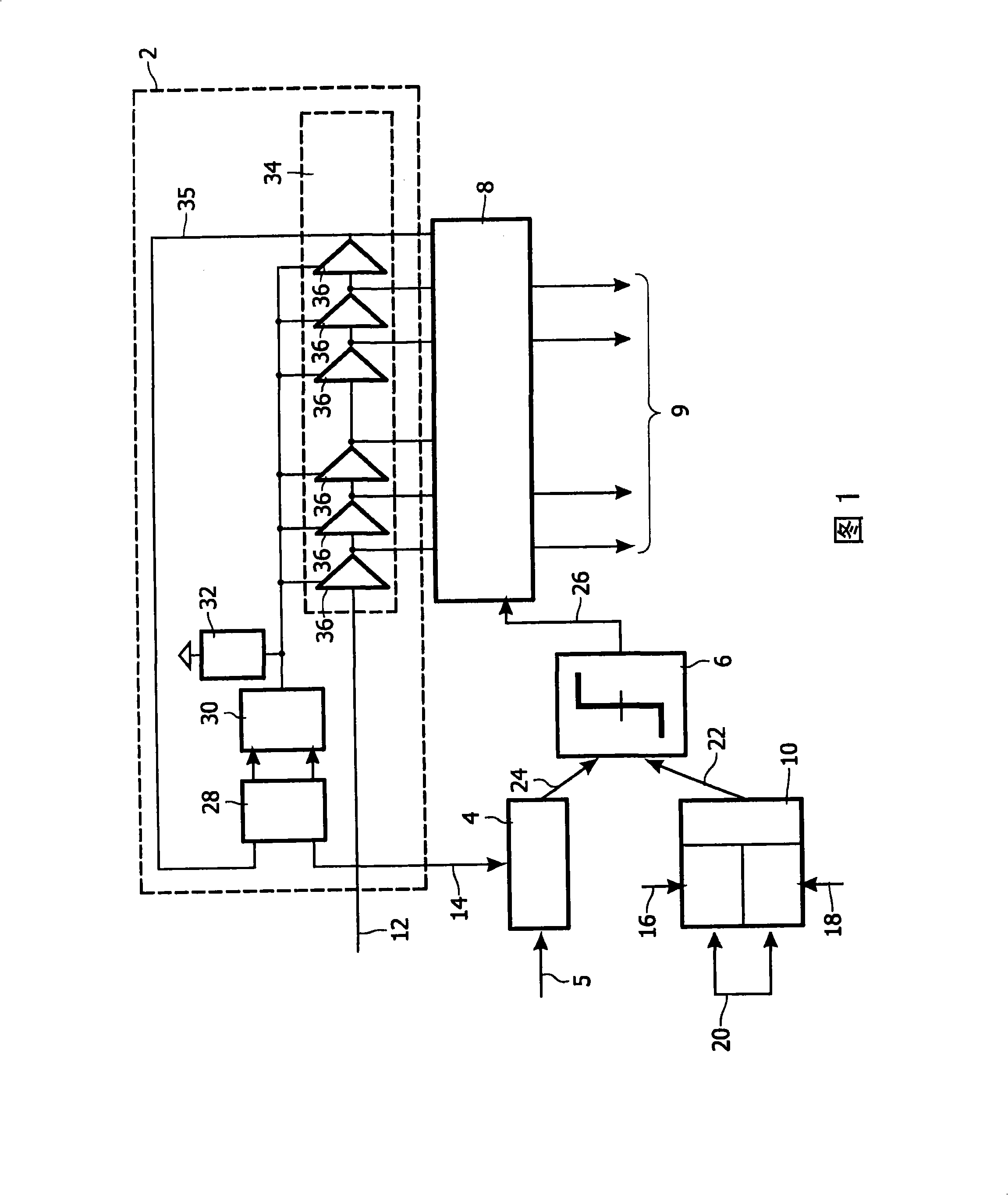
[0041] Fig. 1 depicts a block diagram of an ADC according to a first embodiment of the present invention. The ADC includes a DLL 2 , an integrator 4 , a comparator 6 , a digital logic circuit 8 and a sample and hold module 10 .
[0042] A reference clock source (not shown) generates a reference clock signal, which in this embodiment is a PLL but can also be implemented by other devices such as a crystal oscillator, the frequency of the reference clock signal is f s =1 / T s , where f s is the sampling frequency, T s is the sampling period. For the 180nm CMOS process, the typical sampling frequency is 250MHz, and the resolution is 7 or 8 bits. However, the speed can be increased according to technical standards. The reference clock signal is connected to the input 12 of the DLL 2 as well as to the reset input 14 of the integrator 4 and the control input of the sample and hold module 10 . The inversion of the reference clock signal is provided to the control input 16 of the ...
PUM
 Abstract
Description
Claims
Application Information
 - R&D
- Intellectual Property
- Life Sciences
- Materials
- Tech Scout
- Unparalleled Data Quality
- Higher Quality Content
- 60% Fewer Hallucinations
Browse by: Latest US Patents, China's latest patents, Technical Efficacy Thesaurus, Application Domain, Technology Topic, Popular Technical Reports.
© 2025 PatSnap. All rights reserved.Legal|Privacy policy|Modern Slavery Act Transparency Statement|Sitemap|About US| Contact US: help@patsnap.com