
Peak detection circuit integrated on CMOS single chip

An oxide semiconductor, peak detection circuit technology, applied in single semiconductor device testing, semiconductor/solid-state device testing/measurement, AC/pulse peak measurement, etc., can solve problems such as parasitic parameters, leakage, complex circuit structure, etc., to simplify requirements, reducing volume power consumption, and the effect of high resolution

Active Publication Date: 2008-09-24
INST OF ELECTRONICS CHINESE ACAD OF SCI
View PDF0 Cites 17 Cited by
  • Summary
  • Abstract
  • Description
  • Claims
  • Application Information

AI Technical Summary

Problems solved by technology

[0003] In order to solve the problems of complex circuit structure, parasitic parameters and leakage in the prior art, the purpose of the present invention is to reduce volume power consumption and the needs of sensor and circuit integration, and propose a peak value of complementary metal oxide semiconductor (CMOS) monolithic integration detection circuit

Method used


Image

  • Peak detection circuit integrated on CMOS single chip
  • Peak detection circuit integrated on CMOS single chip
  • Peak detection circuit integrated on CMOS single chip

Examples


Embodiment Construction

[0033] The present invention will be described in detail below in conjunction with the accompanying drawings. It should be noted that the described embodiments are only intended to facilitate the understanding of the present invention, rather than limiting it in any way.

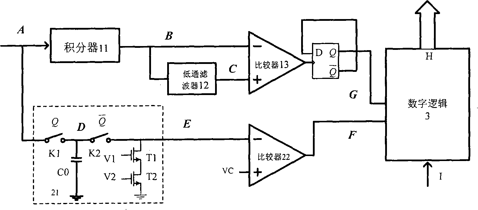
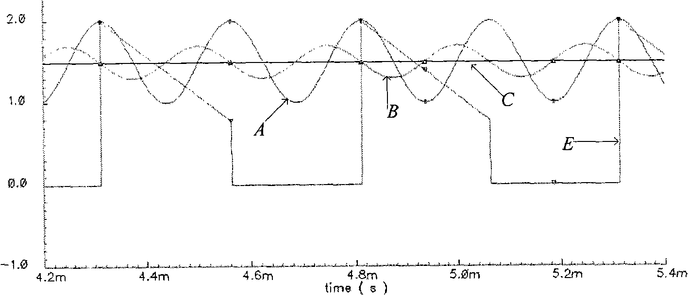
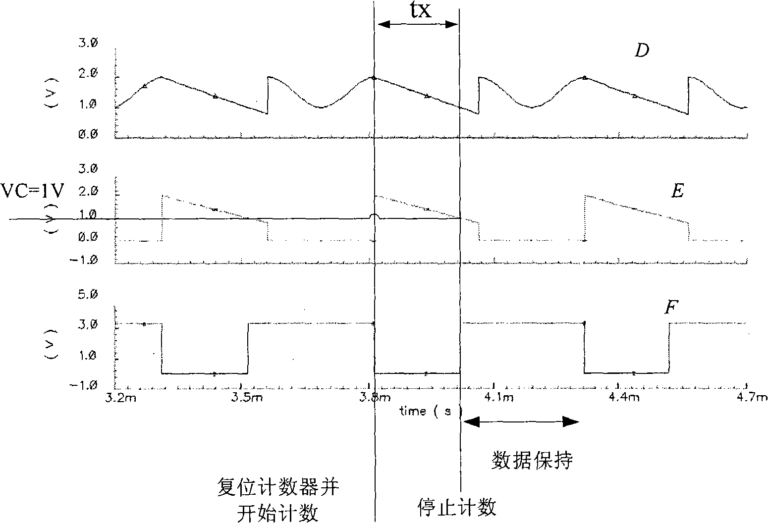
[0034] Specific circuit such as figure 1 As shown in the overall block diagram of the peak detection circuit, the circuit is divided into three parts: peak point finding circuit 1, peak point discharge circuit 2 and digital logic 3, of which:

[0035] One, select the concrete form of peak point finding circuit 1 to comprise: integrator 11, low-pass filter 12, first comparator 13, flip-flop D, wherein:

[0036] Integrator 11, the input sinusoidal signal A passes through the integrator 11, and is divided into two ways to output the integrated signal B; the specific form that the integrator 11 can adopt is as follows Figure 5 Shown: including the first resistor Rf, capacitor C, resistor R, resistor Rp, and th...


PUM


Abstract

The invention pertains to the technical field of complementary metal-oxide semiconductors, which discloses a complementary metal-oxide semiconductor monolithic integrated peak value detection circuit, comprising: a peak value point seeking circuit which is used for generating a rising edge signal at the time of inputting the peak value point of a sine wave signal A; a peak value point discharge circuit which is used for generating a discharge waveform signal E at the site of inputting the peak value point of the sine wave signal; a digital logic, a digital frequency division signal G and a digital waveform signal F are used for controlling the counting of time intervals of an external clock input I, thus generating a digital output signal H of the characteristic time intervals. The circuit of the invention only carries out the sampling of the peak value point, thus simplifying the requirements on a sampling circuit. The peak value detection circuit utilizes the voltage-time conversion (or voltage-duty ratio conversion); the circuit resolution of the invention is controlled by the frequency of a counting clock, thus being much higher than the resolution of the ordinary analog-to-digital converter with the same digital number. The peak value detection circuit can reduce the volume power consumption and meet the needs of the integration of a sensor and the circuits.

Description

technical field [0001] The invention belongs to the technical field of complementary metal oxide semiconductors, and in particular relates to peak detection of monolithic integration of complementary metal oxide semiconductors. Background technique [0002] The peak detection circuit is the basic module in the analog circuit, which is widely used in optical receivers【1】(Ja-Won Sm, Sub Han, Sang-Gug Lee, Man-Seop Lee and Tae Whan Yoo, A1.25Gb / s High Sensitive Peak Detector in Optical Burst-Mode Receiver Using a0.18u.m CMOS Technology, Proceedings of 2003International Conference on Communication Technology, Volume 1, 9-11April 2003, Page(s): 644-646), servo mechanism of hard disk drive【2】( Krhishnaswamy Nagaraj, Stephen H. Lewis, Robert W. Walden, AMedian Peak Detecting Analog Signal Processor for Hard Disk DriveServo, IEEE Journal of Solid-State Circuits, Volume 30 Issue 4, April1995, Page(s): 461-470), generally Sine wave peak detection adopts the method of correlation dete...

Claims


Application Information

Patent Timeline
Patent Type & Authority Applications(China)
IPC IPC(8): G01R31/26G01R31/28G01R19/04H01L21/66
Inventor 杨海钢崔国平
Owner INST OF ELECTRONICS CHINESE ACAD OF SCI
Learn More