Method for desorption of silicon slice

A silicon wafer and desorption technology, applied in electrical components, semiconductor/solid-state device manufacturing, circuits, etc., can solve the problems of low desorption safety of silicon wafers, unfavorable process integration and improve productivity, etc., to achieve high production efficiency, The effect of eliminating residual charge and high process integration

Active Publication Date: 2010-07-21
BEIJING NAURA MICROELECTRONICS EQUIP CO LTD
View PDF6 Cites 0 Cited by
  • Summary
  • Abstract
  • Description
  • Claims
  • Application Information

AI Technical Summary

Problems solved by technology

[0004] In the prior art, the charge elimination inside the electrostatic chuck, the charge elimination on the surface of the silicon wafer, and the detection of whether the charge elimination is complete are all carried out step by step, which is not conducive to process integration and improvement of productivity, and the safety of silicon wafer desorption Sex is not high

Method used


Image

  • Method for desorption of silicon slice
  • Method for desorption of silicon slice

Examples


Embodiment Construction

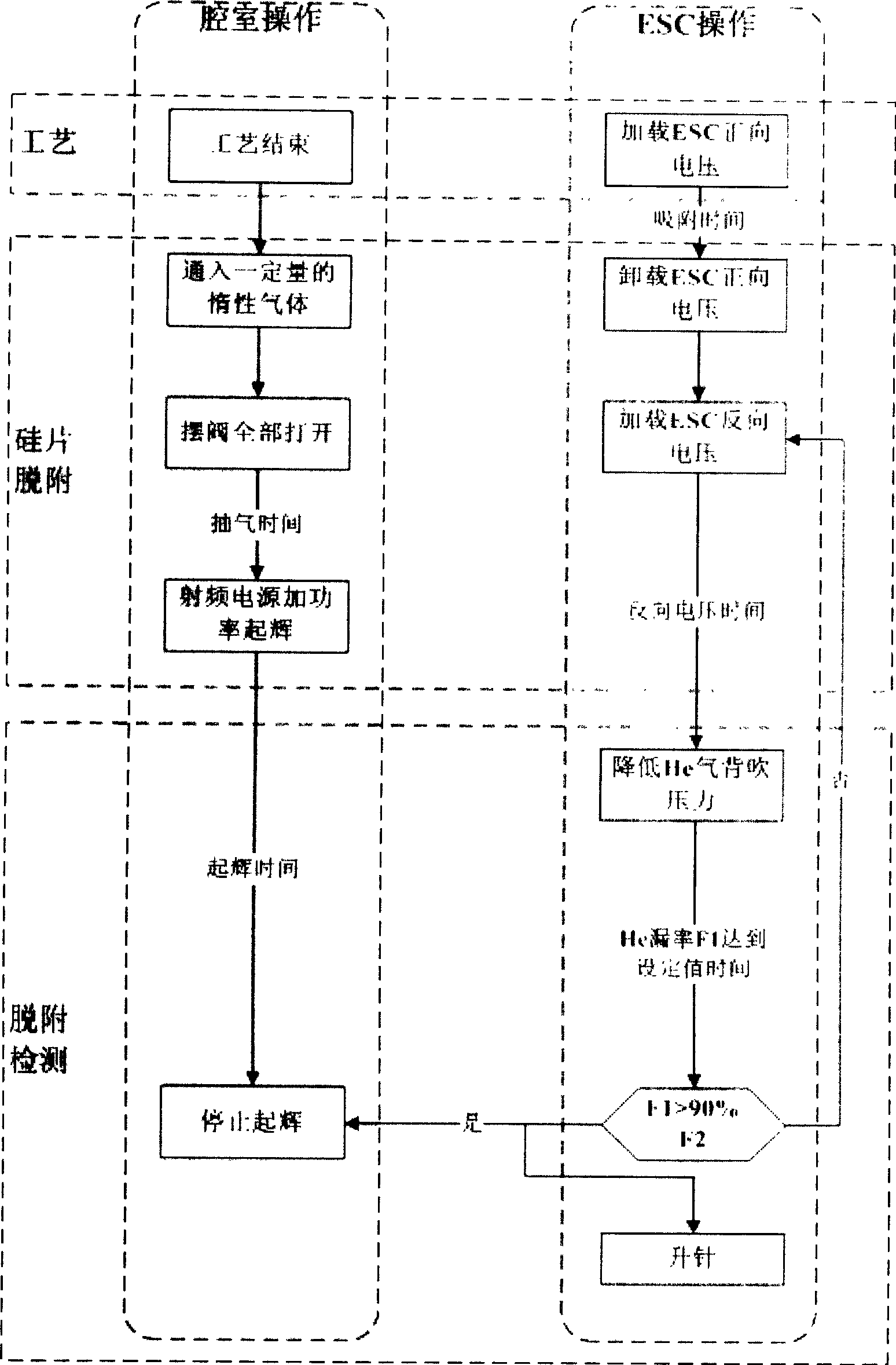
[0024] The preferred embodiment of the method for silicon wafer desorption of the present invention is as follows: figure 1 shown, including

[0025] Step 11. Remove the forward voltage of the electrostatic chuck and increase the reverse voltage to the ESC (electrostatic chuck). The main function of this step is to eliminate the static charge inside the electrostatic chuck by increasing the reverse voltage.

[0026] Step 12: Introduce an inert gas into the reaction chamber, and turn on the radio frequency source to ionize the inert gas into plasma. The main function of this step is to use the conductivity of ions to eliminate the residual charge on the surface of the silicon wafer. At the same time, the residual charge on the surface of the electrostatic chuck is also eliminated.

[0027] Step 13. Judging whether the silicon wafer is desorbed according to the leakage flow rate of the back-blown He gas on the back of the silicon wafer from between the silicon wafer and the ele...


PUM


Abstract

The invention discloses a desorption method of silicon chips, which comprises initially increasing backward voltage to an electrostatic chuck for removing electrostatic charge inside the electrostatic chuck, simultaneously removing residual electric charge on the surface of the silicon chips through ionizing inert gas into plasmas by employing the electrical conductivity of ions and judging whether the silicon chips are completely desorbed through the leakage flow rate of back blowing He gas of the back face of the silicon chips between the silicon chips and the electrostatic chuck. The invention has the advantages of high technical integration, safety and high production efficiency, and is particularly adaptable to desorption between the silicon chips and the electrostatic chuck in the processing technique of semiconductor silicon chips.

Description

technical field [0001] The invention relates to a semiconductor silicon chip processing technology, in particular to a silicon chip desorption method. Background technique [0002] In the silicon wafer dry etching process, the silicon wafer is generally placed on the ESC (electrostatic chuck) in the reaction chamber for the etching process. Generally, a forward voltage is applied to the electrostatic chuck, and the silicon wafer is attracted by electrostatic attraction. Adsorbed on the electrostatic chuck. After the etching is completed, the silicon wafer should be desorbed, that is, the residual charge inside the electrostatic chuck and the surface of the silicon wafer should be eliminated, so that the silicon wafer can be completely separated from the electrostatic chuck. The smooth desorption of silicon wafers plays a vital role in the stable productivity of the etching process itself and the etching process. Silicon wafer desorption mainly includes two aspects: the eli...

Claims


Application Information

Patent Timeline
Patent Type & Authority Patents(China)
IPC IPC(8): H01L21/00H01L21/67H01L21/683H01L21/306H01L21/3065C23F4/00
Inventor 彭东阳
Owner BEIJING NAURA MICROELECTRONICS EQUIP CO LTD
Why Eureka
Try Eureka