Plasma display device

A plasma and display device technology, applied in the direction of identification devices, electronic switches, static indicators, etc., can solve the problems of driving waveform information changes, useless through current, control signal influence, etc., and achieve the effect of preventing the generation of through current

Inactive Publication Date: 2008-07-23
FUJITSU HITACHI PLASMA DISPLAY LTD
View PDF1 Cites 0 Cited by
  • Summary
  • Abstract
  • Description
  • Claims
  • Application Information

AI Technical Summary

Problems solved by technology

[0008] However, when the wiring structure described in the aforementioned Japanese Patent Application Laid-Open No. 2005-300568 is adopted, the length of the wiring for transmitting the driving waveform information signal becomes longer, and it is expected that the driving waveform information will change due to noise.
Since the wiring of the driving waveform information signal is usually composed of multi-bit signal lines, the inversion of any bit due to noise will cause a large change in the driving waveform information, and the control signal generated by the front-stage driving circuit will also be affected. will have a big impact
[0009] On the other hand, the main drive circuit of the above-mentioned electrode drive circuit is composed of a plurality of switching transistors for power recovery, but when these switches are improperly turned on, a useless through current will be generated.

Method used


Image

  • Plasma display device
  • Plasma display device
  • Plasma display device

Examples


Embodiment Construction

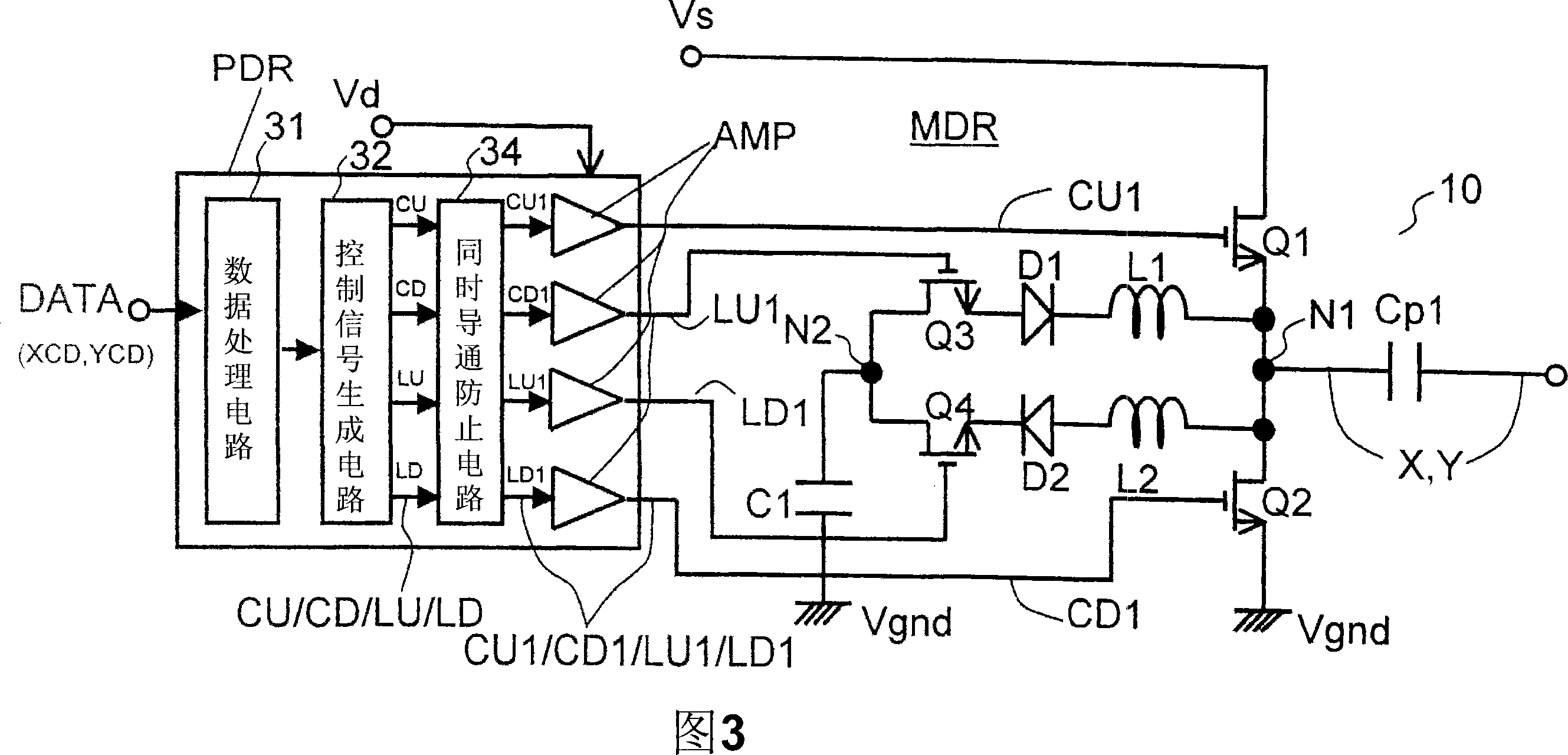
[0037] Hereinafter, embodiments of the present invention will be described based on the drawings. However, the technical scope of the present invention is not limited to these embodiments, and includes matters described in the claims and their equivalents.

[0038] FIG. 1 is a configuration diagram of a plasma display device according to this embodiment. The plasma display device has: a plasma display panel 10 having a plurality of display electrodes X, Y extending in the horizontal direction, and a plurality of address electrodes A extending in the vertical direction intersecting the display electrodes X, Y; The unit 20 is driven by applying a driving pulse to the electrodes of the panel; the input signal processing circuit 30 performs image processing on the video signal IN input from a TV tuner (television tuner), DVD player, etc., to generate a plasma display panel. image signal. The input signal processing circuit generates, for example, an image digital signal for each...


PUM


Abstract

In the plasma display device, an electrode drive unit has a main drive circuit applying a drive pulse, a pre-drive circuit supplying control signals to the main drive circuit, and a drive control circuit supplying a drive waveform information signal to the pre-drive circuit. The main drive circuit has switches for generating the drive pulse and a charge collection capacitor. The pre-drive circuit has a control signal generation circuit which generates first to fourth control signals for controlling the first to fourth switches based on the drive waveform information signal, and a simultaneous ON prevention circuit which disables a set of the first and second, the first and fourth, and the second and third control signals to be a simultaneous ON control state respectively.

Description

technical field [0001] The present invention relates to a plasma display device, and more particularly, to a plasma display device that prevents malfunction of a drive circuit that drives display electrodes. Background technique [0002] A plasma display device has a plurality of display electrodes (X, Y electrodes) extending in the horizontal direction and a plurality of address electrodes intersecting the display electrodes, and has a driving circuit for driving each electrode. Plasma display devices that are popular now generally adopt an Address Display-period Separated (ADS) driving method. [0003] In the ADS drive method, the drive control includes an address period in which display data is written from the address electrodes while scanning the display electrodes, and a sustain period in which voltages are alternately applied to the display electrode pairs after the address period. In particular, a sustain pulse is repeatedly applied to the same display electrode in ...

Claims


Application Information

Patent Timeline
Patent Type & Authority Applications(China)
IPC IPC(8): G09G3/28H03K17/13H03K17/687H01J17/49G09F9/313G09G3/288G09G3/20G09G3/291G09G3/294G09G3/296G09G3/298
CPCG09G3/2965G09G3/296
Inventor 小野泽诚岸智胜
Owner FUJITSU HITACHI PLASMA DISPLAY LTD
Why Eureka
Try Eureka