Flat-panel display device and driving method thereof

A technology of flat-panel display and driving method, which is applied to static indicators, instruments, etc., and can solve the problems of inconsistency in charge coupling between odd-numbered pixels and even-numbered pixels, traces in the vertical direction, uneven brightness of image screens, etc.

Active Publication Date: 2008-07-16
AU OPTRONICS CORP
View PDF0 Cites 9 Cited by
  • Summary
  • Abstract
  • Description
  • Claims
  • Application Information

AI Technical Summary

Problems solved by technology

In this way, the charging coupling degree of odd-numbered pixels and even-numbered pixels is inconsistent, resulting in traces in the vertical direction of the image due to uneven brightness

Method used


Image

  • Flat-panel display device and driving method thereof
  • Flat-panel display device and driving method thereof
  • Flat-panel display device and driving method thereof

Examples


no. 1 example

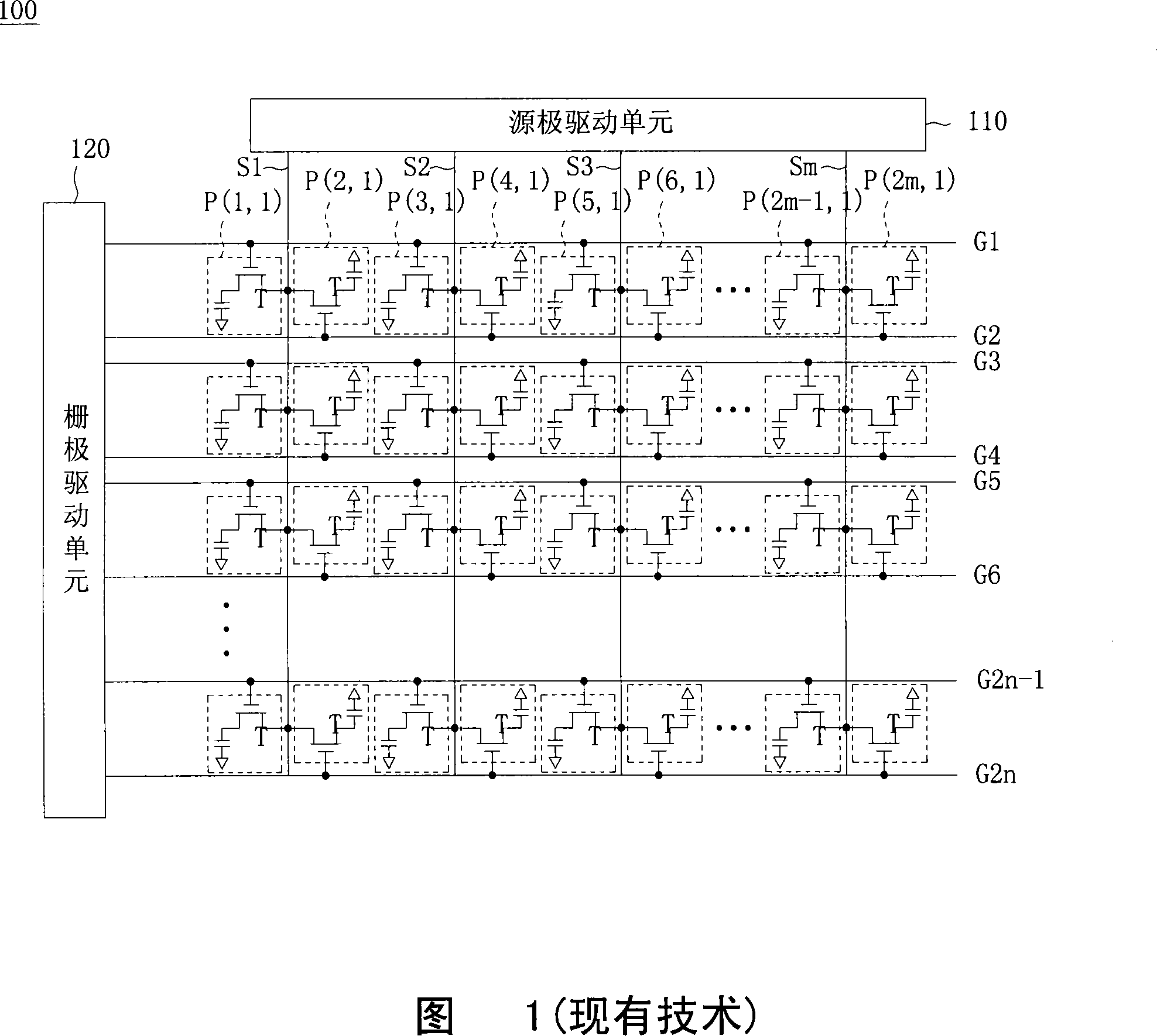
[0027] FIG. 2A is a schematic diagram of the first embodiment of the liquid crystal display of the present invention. As shown in FIG. 2A, the liquid crystal display 200 includes a substrate (not shown in the figure), a plurality of data lines S1-Sm, a plurality of scan lines G1-G2n, a source driving unit 210 and a gate driving unit 220, m and n is a positive integer. The substrate is, for example, a glass substrate, which includes the pixel array 230 . The pixel array 230 includes a plurality of pixels P(x, y), x and y are positive integers, and each pixel includes a transistor T. In the flat panel display 200 , each data line S1 -Sm is electrically connected to two transistors of two adjacent pixels in each row of pixels, for example.

[0028] A plurality of data lines S1˜Sm are electrically connected to the pixel array 230 . A plurality of scanning lines G1-G2n are electrically connected to the pixel array 230, and these scanning lines G1-G2n include a plurality of odd-n...

no. 2 example

[0046] FIG. 4A is a schematic diagram of a second embodiment of the liquid crystal display of the present invention. The liquid crystal display 400 includes a substrate (not shown in the figure), a plurality of data lines S1˜Sm, a plurality of scan lines G1˜G2n, a source driving unit 410 and a gate driving unit 420, where m and n are positive integers. The substrate is, for example, a glass substrate, which includes a pixel array 430 . The pixel array 430 includes a plurality of pixels, and each pixel includes a transistor (not shown in the figure). In the liquid crystal display 400 , each data line S1 ˜Sm is electrically connected to p transistors of each column of pixels, and p is a positive integer.

[0047] A plurality of data lines S1˜Sm are electrically connected to the pixel array 430 . A plurality of scan lines G1-G2n are electrically connected to the pixel array 430, and these scan lines G1-G2n include p groups of scan lines, wherein at least some of the scan lines ...


PUM


Abstract

A flat panel display comprises a substrate, a plurality of data lines, a plurality of scan lines, a source electrode driver element and a grid electrode driver element. The substrate comprises a pixel array. The plurality of data lines are electrically connected to the pixel array. The plurality of scan lines comprise p groups of scan lines and are electrically connected with the pixel array, and P is a positive integer. In the same group of the scan lines, at least partial scan lines are not adjacent. The source electrode unit is electrically connected to the partial scan lines. The grid electrode driver element comprises p shift register circuits which are respectively used to enable the p groups of scan lines. In a first picture frame period, the p groups of scan lines are enabled by a first group sequence; in a second picture frame period, the p groups of scan lines are enabled by a second group sequence, and the first group sequence is different from the second group sequence.

Description

【Technical field】 [0001] The present invention relates to a flat-panel display and a driving method thereof, in particular to a flat-panel display capable of improving image quality and a driving method thereof. 【Background technique】 [0002] Nowadays, the technology of flat panel displays develops rapidly, and various technologies are continuously developed. In order to reduce the number of integrated circuit (IC) signal lines to save costs, some non-traditional panel charging circuit architectures have emerged in the technical field of the present invention. However, in these panel charging architectures, since the circuit layout of each pixel is different from the traditional circuit layout, various traces (mura) will be generated on the picture, thereby affecting the image quality of the picture. [0003] Figure 1 is a schematic diagram of a conventional liquid crystal display. As shown in FIG. 1, the liquid crystal display 100 includes a substrate (not shown in the f...

Claims


Application Information

Patent Timeline
Patent Type & Authority Applications(China)
IPC IPC(8): G09G3/20G09G3/36G02F1/133
Inventor 李忠隆刘匡祥王仓鸿
Owner AU OPTRONICS CORP
Why Eureka
Try Eureka