Combined test action group test system of micro-electric communication processing structure
A technology of joint test action and test system, applied in the direction of digital circuit test, electronic circuit test, etc., can solve the problems of increasing the complexity of the backplane, increasing the manufacturing cost of the JTAG test system, etc., and achieve the effect of reducing the manufacturing cost
Inactive Publication Date: 2010-11-10
丛云鹏
View PDF0 Cites 0 Cited by
- Summary
- Abstract
- Description
- Claims
- Application Information
AI Technical Summary
Problems solved by technology
Then, if JSM is implemented on the backplane, the complexity of the backplane will be increased, and a placement process will be added during processing.
If an additional single board is used to implement JSM, it will inevitably increase the manufacturing cost of MicroTCA's JTAG test system
Method used
View moreImage
Smart ImageViewing Examples
Examples
Embodiment Construction
Login to View More PUM
 Abstract
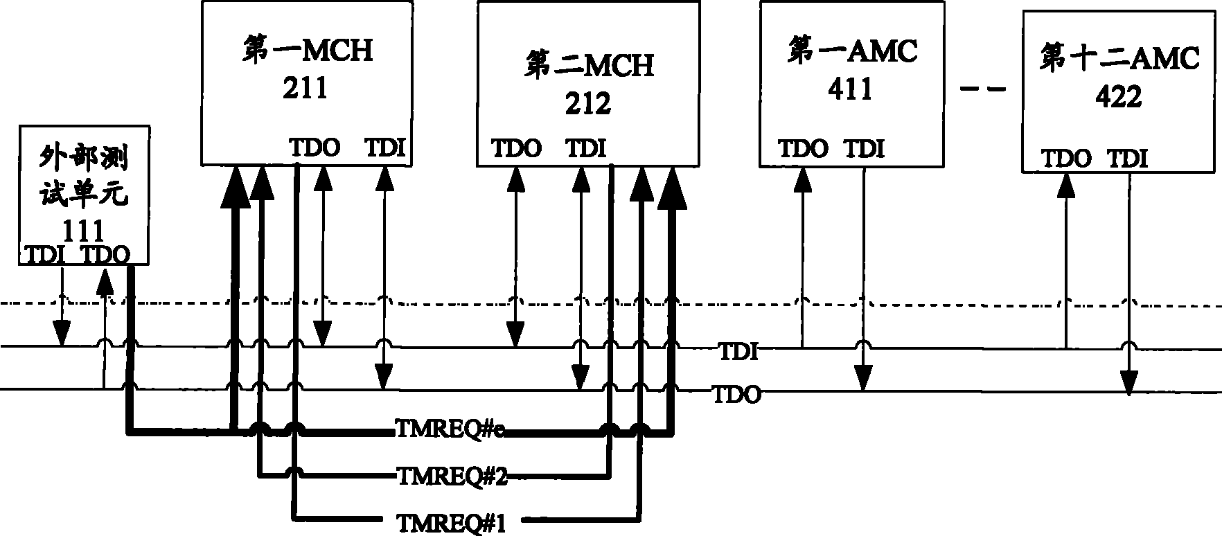
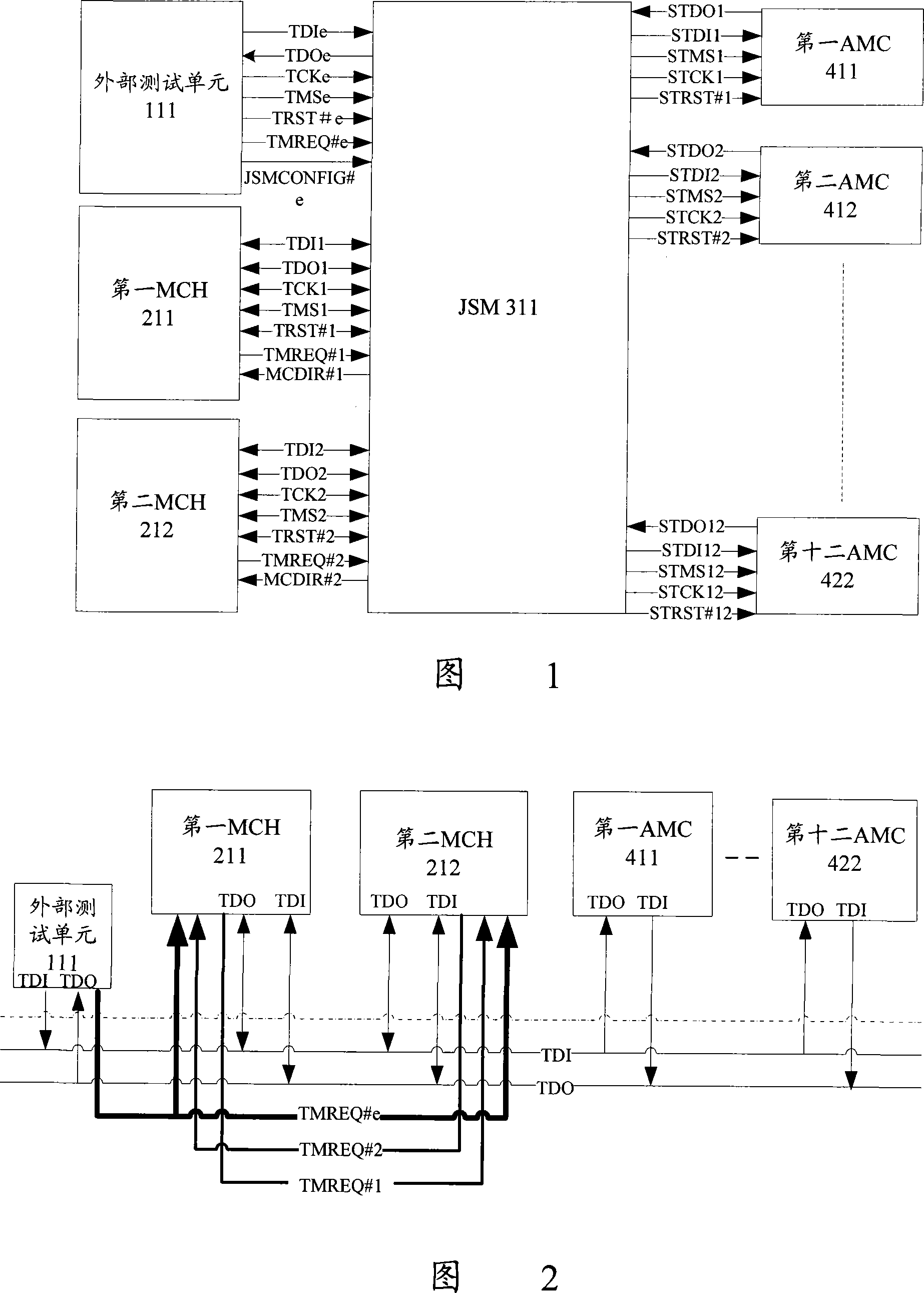
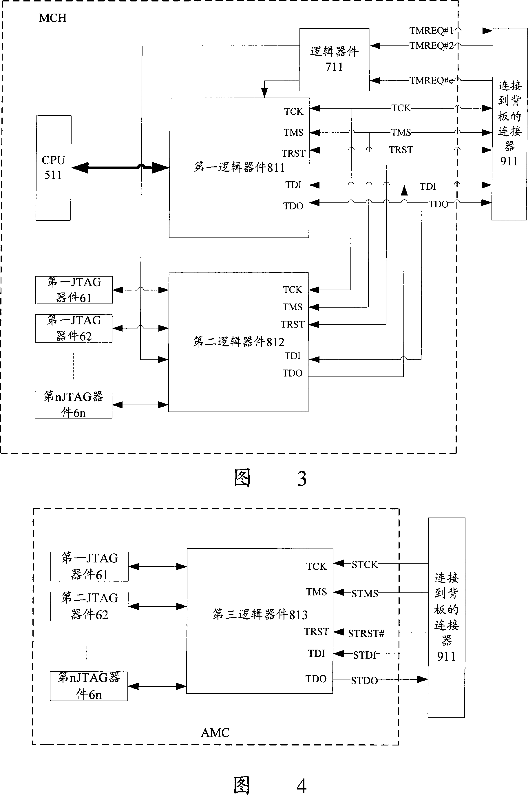
The invention discloses a joint test action group (JTAG) test system of a micro-telecommunication computing architecture, which comprises an external test unit, and main carrier hubs (MCH) and an advanced mezzanine card (AMC) of a micro-telecommunication computing architecture, wherein the external test unit is connected with the JTAG interfaces of the MCH and the AMC in a bus manner to serve as a main device master for testing the MCH and the AMC; the MCH serves as a master for testing the AMC or as a slave to be tested by the external test unit; and the AMC services as a slave to be tested by the current master. The invention can achieve connection between the selected master and the set slave and achieve slave test step by step without achieving JTAG switch module (JSM).
Description
A Joint Test Action Group Test System for Microtelecom Processing Architecture technical field The present invention relates to joint test action group (JTAG, JOINTTESTACTIONGROUP) test technology, particularly relates to a kind of JTAG test system of microtelecommunication processing framework (MicroTCA, MicroTelecommunicationComputingArchitecture). Background technique The JTAG protocol is an international standard test protocol, mainly used for chip internal testing. The PCI Industrial Computer Manufacturers Group (PICMG, PCIIndustrialComputerManufacturersGroup) has developed a set of MicroTCA specifications, the purpose of which is to allow advanced daughter cards (AMC, AdvancedMezzanineCard) to be directly inserted into the backplane. Due to its small size, good scalability and flexibility, and cost factors, MicroTCA is suitable for use in wireless base station side equipment. Test is a more important part of MicroTCA, and the test of MicroTCA can be realized with J...
Claims
Login to View More Application Information
Patent Timeline
 Patent Type & Authority Patents(China)
IPC IPC(8): G01R31/317
Inventor 王强胡浩
Owner 丛云鹏
Features
- R&D
- Intellectual Property
- Life Sciences
- Materials
- Tech Scout
- Unparalleled Data Quality
- Higher Quality Content
- 60% Fewer Hallucinations
Learn More Browse by: Latest US Patents, China's latest patents, Technical Efficacy Thesaurus, Application Domain, Technology Topic, Popular Technical Reports.
© 2025 PatSnap. All rights reserved.Legal|Privacy policy|Modern Slavery Act Transparency Statement|Sitemap|About US| Contact US: help@patsnap.com


