Method for measuring phase delay of crystal broad spectrum
A phase delay and measurement method technology, applied in the field of crystal material measurement, can solve the problems of time-consuming and labor-intensive measurement of crystal phase delay, multi-wavelength testing difficulties, etc.
- Summary
- Abstract
- Description
- Claims
- Application Information
AI Technical Summary
Problems solved by technology
Method used
Image
Examples
Embodiment 1
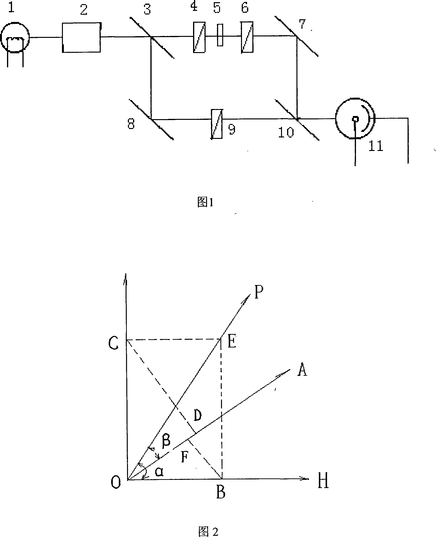
[0043] The embodiment of the present invention is shown in Fig. 1, a kind of device that is used for crystal broad-spectrum phase retardation measuring method, by light source 1, monochromator 2, two reflection mirrors 7,8 and two half mirrors 3,10 , a polarizer 4 and an analyzer 6, a polarizer 9 and a photomultiplier tube 11, the light source 1 is located in front of the monochromator 2, and two reflectors 7, 8 and two semi-transparent and semi-transparent mirrors are placed behind the monochromator 2 Anti-mirror 3,10, can form two parallel optical paths with the monochromatic light that monochromator 2 exits via reflector 8 and half-mirror 3, then by reflector 7 and half-mirror 10 two The light paths are collected into one light path; the photomultiplier tube 11 is placed at the terminal position of the light path of collection, and it is characterized in that a polarizer 4 and an analyzer 6 are sequentially placed in one of the two light paths, and a polarizer 6 is placed in...
Embodiment 2
[0045] This embodiment is shown in Figure 1, a method for measuring the phase delay of a crystal wide spectrum, the steps are as follows:
[0046] a. cutting the measured crystal into wafer samples 5 along the z direction;
[0047] b. In one optical path of the double-beam spectrophotometer, put a polarizer 4 and an analyzer 6, and rotate the analyzer 6 so that its vibration transmission direction is parallel to that of the polarizer 4;
[0048] c. Put a polarizer 9 in another optical path of the double-beam spectrophotometer, adjust the transmission direction of the polarizer 9 to make it the same as the transmission direction of the polarizer 4 in the optical path described in the above step b parallel;
[0049] d. put the wafer sample 5 between the polarizer 4 and the analyzer 6 in the optical path described in the above-mentioned steps b, make its optical axis (e light vibration direction) parallel to the vibration transmission direction of the polarizer 4;
[0050] e. a...
PUM
 Abstract
Description
Claims
Application Information
 - Generate Ideas
- Intellectual Property
- Life Sciences
- Materials
- Tech Scout
- Unparalleled Data Quality
- Higher Quality Content
- 60% Fewer Hallucinations
Browse by: Latest US Patents, China's latest patents, Technical Efficacy Thesaurus, Application Domain, Technology Topic, Popular Technical Reports.
© 2025 PatSnap. All rights reserved.Legal|Privacy policy|Modern Slavery Act Transparency Statement|Sitemap|About US| Contact US: help@patsnap.com


