
Method for reducing stray capacitance in analogue circuit

A parasitic capacitance and analog circuit technology, applied in the field of analog circuit layout design, can solve the problems of reducing current channel, increasing parasitic resistance, slowing down circuit speed, etc.

Inactive Publication Date: 2008-05-07
ZTE CORP
View PDF0 Cites 1 Cited by
  • Summary
  • Abstract
  • Description
  • Claims
  • Application Information

AI Technical Summary

Problems solved by technology

The problem caused by reducing A is that the parasitic resistance on the signal line 3 is increased, and the current channel is reduced, which indirectly causes the speed of the circuit to slow down.

Method used


Image

  • Method for reducing stray capacitance in analogue circuit
  • Method for reducing stray capacitance in analogue circuit
  • Method for reducing stray capacitance in analogue circuit

Examples


Embodiment Construction

[0015] The present invention will be further described below in conjunction with the specific implementation of the method of the present invention.

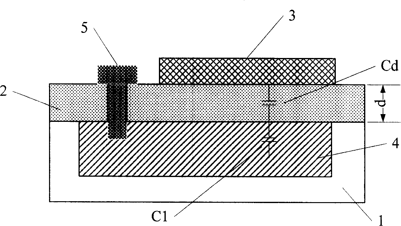
[0016] first refer to figure 2 , which is a cross-sectional view of a signal line and a substrate after adding an N well layer according to an embodiment of the present invention. Taking the semiconductor substrate as a P-type substrate 1 as an example, an N well layer 4 is introduced between the P-type substrate 1 and the insulating layer 2, and the above-mentioned N well layer 4 and the P-type substrate 1 form a capacitor C1, which is connected in series with the original capacitor Cd even. In order to effectively utilize C1 and reduce the original capacitance Cd between the signal line 3 and the substrate, the N well layer 4 must be AC ​​floating (hereinafter referred to as AC floating). If the N well layer 4 is not AC floating, then in the case of alternating current (hereinafter referred to as AC), the potentials of the ...


PUM


Abstract

The invention relates to a method for reducing the parasitic capacitance in analog circuit, which comprises the following steps: an insulation layer is grown on the semiconductor substrate; then a signal line is prepared on the insulation layer, wherein, an N well layer is introduced before growing the insulation layer and is arranged between the insulation layer and the semiconductor substrate. The invention has the advantages that the parasitic capacitance is reduced without increasing the layout area simultaneously, that is, the parasitic capacitance of signal is reduced without increasing the circuit cost.

Description

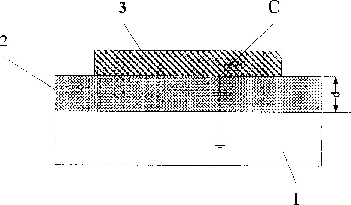
technical field [0001] The invention relates to the field of analog circuit layout design, in particular to a method for reducing parasitic capacitance in an analog circuit. Background technique [0002] The invention is mainly applied in the layout design of analog integrated circuits and in the realization of semiconductor devices. In the process of physical realization of analog circuits, the parasitic capacitance devices on some signal lines usually greatly affect the performance of the circuit, especially for some sensitive high-frequency signals, the influence of parasitic capacitance is more obvious. The parasitic capacitance on the signal line will increase the load, reduce the operating frequency and narrow the operating bandwidth, and will be coupled to the signal line, degrading the anti-interference ability of the signal. Traditional design methods such as figure 1 shown. A layer of insulating layer 2 is grown on the P-type substrate 1, above which is the sign...

Claims


Application Information

Patent Timeline
Patent Type & Authority Applications(China)
IPC IPC(8): H01L21/822H01L21/768H01L27/04
Inventor 李梅林满院周莉吴小晔
Owner ZTE CORP
Learn More