
Stack type metal-oxide-metal capacitor structure

A metal capacitor and oxide technology, applied in capacitors, electric solid devices, circuits, etc., can solve the problem of occupying semiconductor area and volume, and achieve the effect of large capacitance value

Inactive Publication Date: 2008-04-23
TAIWAN SEMICON MFG CO LTD
View PDF0 Cites 14 Cited by
  • Summary
  • Abstract
  • Description
  • Claims
  • Application Information

AI Technical Summary

Problems solved by technology

[0006] Problems with existing technologies include utilizing a large number of stacked metallization layers and associated interconnection vias to achieve the required level of capacitance, thus occupying valuable semiconductor area and volume

Method used


Image

  • Stack type metal-oxide-metal capacitor structure
  • Stack type metal-oxide-metal capacitor structure
  • Stack type metal-oxide-metal capacitor structure

Examples


Embodiment Construction

[0048] In order to further explain the technical means and effects that the present invention takes to achieve the intended purpose of the invention, below in conjunction with the accompanying drawings and preferred embodiments, the specific implementation, structure, Features and their functions are described in detail below.

[0049] While the metal-oxide-metal capacitor structures and methods of fabrication of the present invention are described with reference to exemplary damascene structures, it will be appreciated that these damascene structures can be fabricated using conventional single or dual damascene processes.

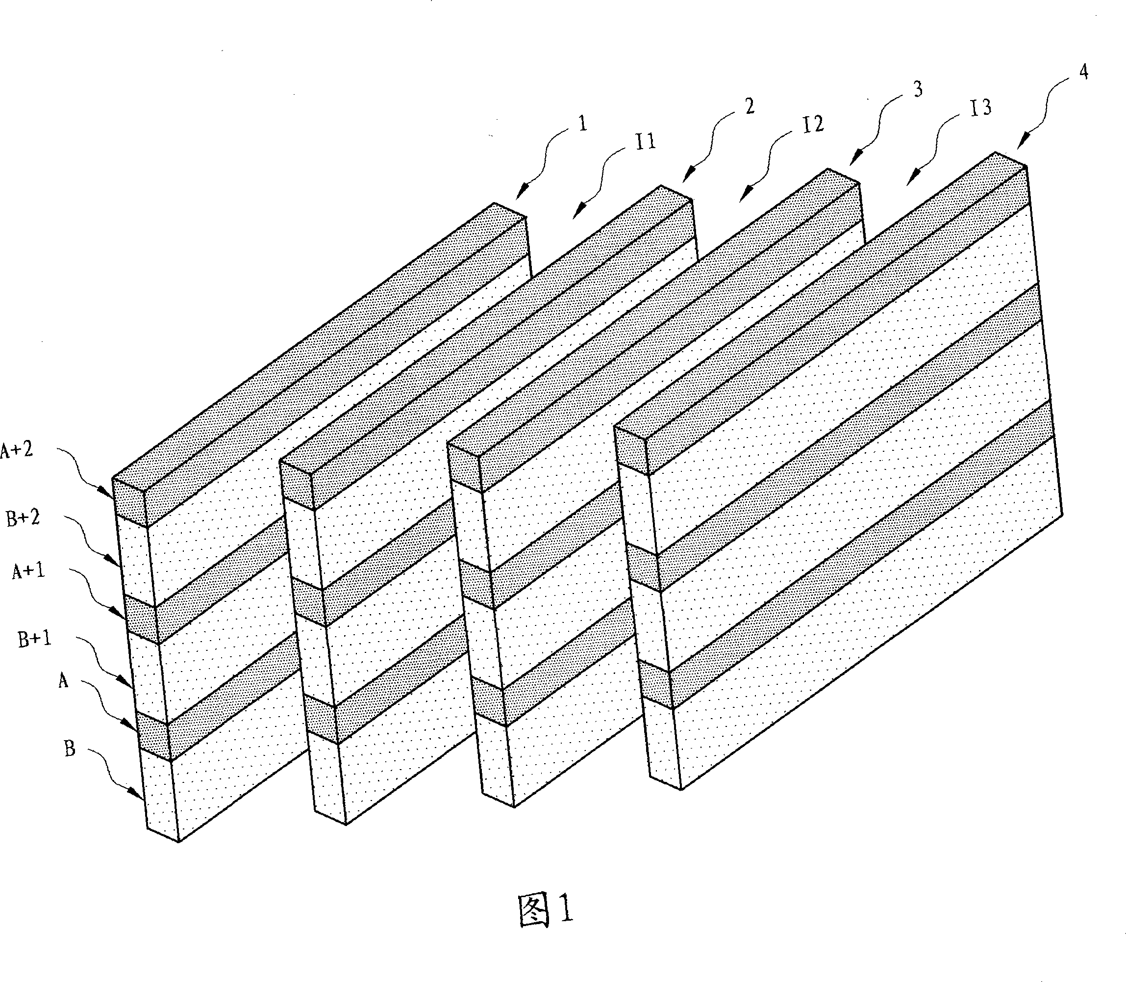
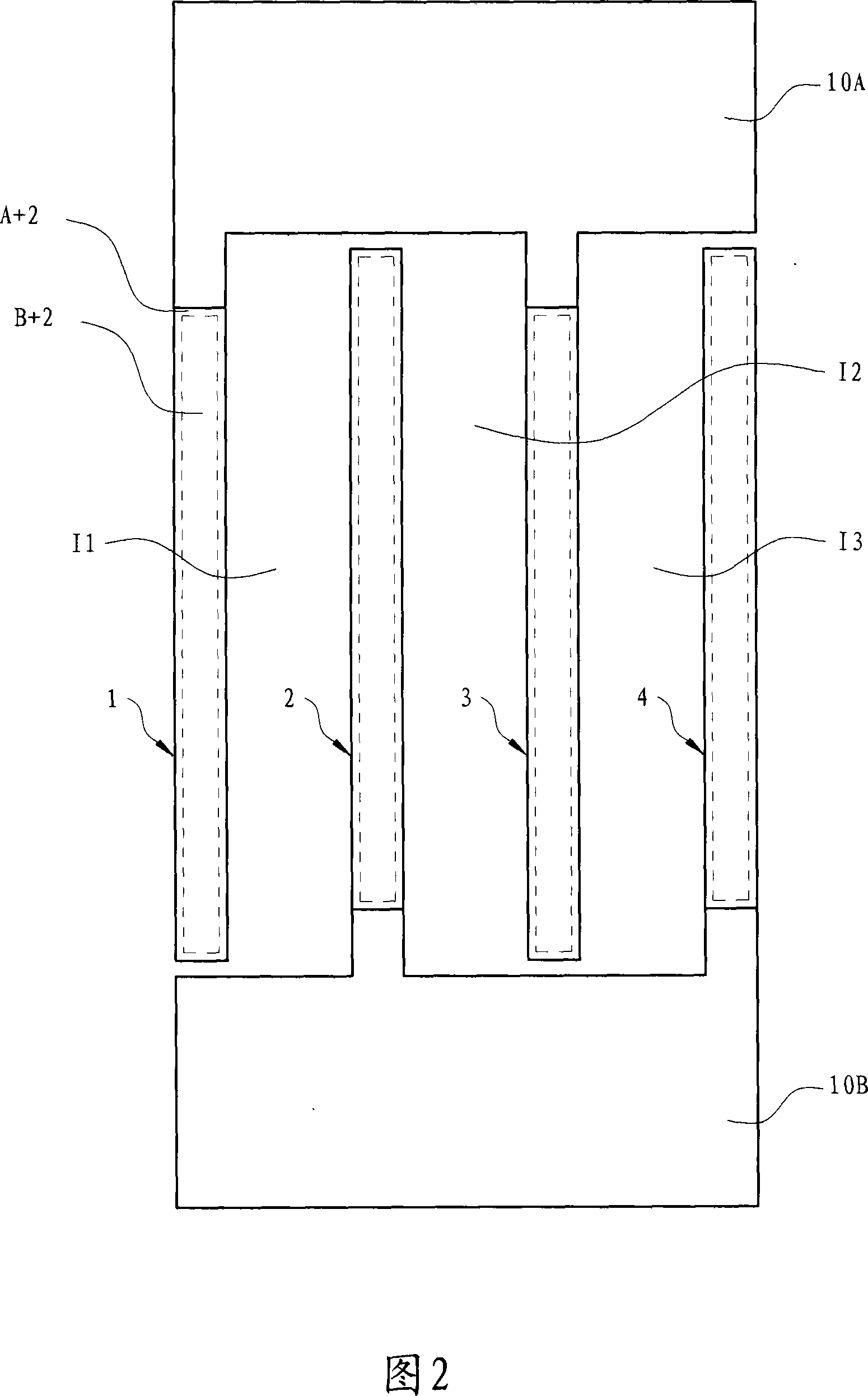
[0050] Please refer to FIG. 1 , which shows a perspective view of an exemplary stacked metallization structure, which only shows the metal part, so as to more properly illustrate the metal-oxide-metal capacitor structure of the present invention. It will be appreciated that one or more capacitor dielectric materials, such as dielectric materials I1, I2 and...


PUM


Abstract

A stacked metal-oxide-metal (MOM) capacitor structure and method of forming the same to increase an electrode / capacitor dielectric coupling area to increase a capacitance, the MOM capacitor structure including a plurality of metallization layers in stacked relationship; wherein each metallization layer includes substantially parallel spaced apart conductive electrode line portions having a first intervening capacitor dielectric; and, wherein the conductive electrode line portions are electrically interconnected between metallization layers by conductive damascene line portions formed in a second capacitor dielectric and disposed underlying the conductive electrode line portions.

Description

technical field [0001] The present invention relates to a metal-oxide-metal (MOM) capacitor structure, in particular to a mosaic stacked metal-oxide-metal capacitor structure and its manufacturing method, wherein the mosaic stacked metal-oxide-metal capacitor The structure includes a simplified layout, and the fabrication method includes forming the metal-oxide-metal structure with increased capacitive coupling area to increase the capacitance of the metal-oxide-metal structure. Background technique [0002] The development of technology has continuously increased the demand for System-on-chip (SoC) products, wherein in the System-on-chip products, both analog and digital signals can be processed satisfactorily. For example, an analog circuit captures an analog signal from the surrounding environment, converts the analog signal into bits, and then converts the bits into signals to drive a digital circuit to generate functions. There is an increasing advantage in placing ana...

Claims


Application Information

Patent Timeline
Patent Type & Authority Applications(China)
IPC IPC(8): H01L29/92H01L23/522H01L27/00
CPCH01L2924/0002H01L23/5223H01L28/60H01L2924/3011H01L2924/00
Inventor 陈朝祺金明铸周振成
Owner TAIWAN SEMICON MFG CO LTD
Learn More