Plasma etching method and device

An etching device and plasma technology, used in the manufacture of electrical components, discharge tubes, semiconductor/solid-state devices, etc., can solve the problems of difficulty in controlling the depth of the LDD region and affect device performance, and achieve the effect of eliminating dents and improving control accuracy.

Active Publication Date: 2008-04-02
SEMICON MFG INT (SHANGHAI) CORP +1
View PDF1 Cites 24 Cited by
  • Summary
  • Abstract
  • Description
  • Claims
  • Application Information

AI Technical Summary

Problems solved by technology

However, for devices with a thickness of 65nm and below, the thickness of the gate oxide layer is only about 10 Ȧ. The above-mentioned depressions caused by the loss of silicon will make it difficult to control the depth of the LDD region, seriously affecting device performance.

Method used


Image

  • Plasma etching method and device
  • Plasma etching method and device
  • Plasma etching method and device

Examples


Embodiment Construction

[0037] In order to make the above objects, features and advantages of the present invention more comprehensible, specific implementations of the present invention will be described in detail below in conjunction with the accompanying drawings.

[0038] In the following description, numerous specific details are set forth in order to provide a thorough understanding of the present invention. However, the present invention can be implemented in many ways other than those described here, and those skilled in the art can make similar extensions without departing from the connotation of the present invention. Accordingly, the invention is not limited to the specific implementations disclosed below.

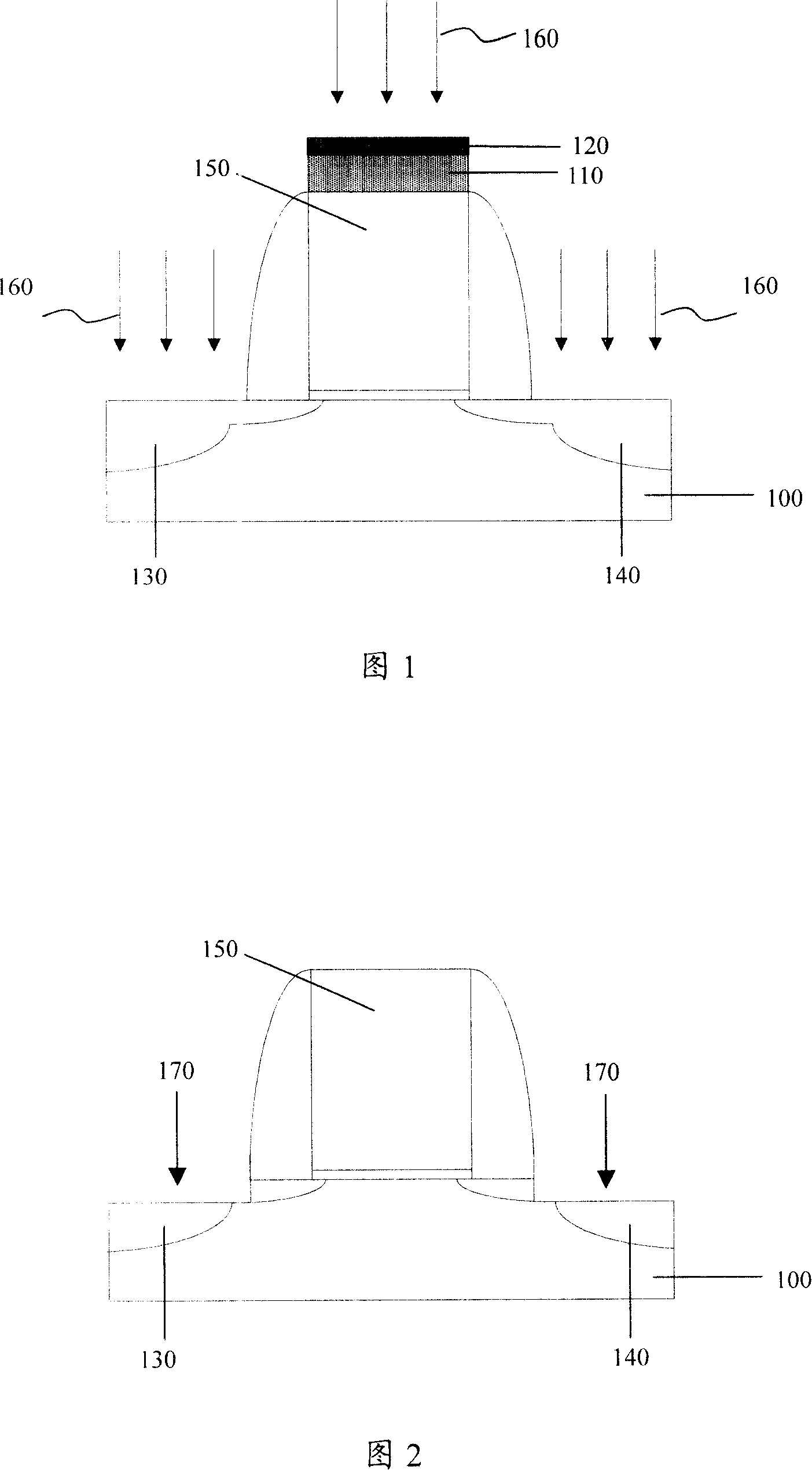
[0039] The plasma etching process is an important process in semiconductor manufacturing technology, such as the etching of dielectric layers, which include silicon oxide layers, silicon nitride layers, polysilicon layers, etc., as well as hafnium oxide, hafnium silicon oxide and hafni...


PUM


Abstract

The invention discloses a plasma etching method and device, wherein, the method includes the following steps: the inside of a reaction chamber is provided with a semiconductor substrate which is provided with a to-be-etched material layer; etching gas which is ionized into plasma by a radio frequency power source is fed in the reaction chamber; the radio frequency power source outputs radio frequency power in pulse output mode. The device comprises a reaction chamber, a wafer holder, a first radio frequency power source, a loop winding, a second radio frequency power source and a pulse control circuit, wherein, the inside of the reaction chamber contains the etching gas; the wafer holder is used to bear the weight of a semiconductor wafer; the first radio frequency power source provides bias voltage for the wafer; the loop winding is arranged at the upper part and the top of the reaction chamber; the second radio frequency power source which is used to generate radio frequency power is connected with the loop winding through the pulse control circuit and outputs radio frequency power in pulse output mode to ionize the etching gas into plasma. The invention can generate plasma which is output in pulse mode and used for etching, thereby improving the control precision of etch end point.

Description

technical field [0001] The invention relates to the technical field of semiconductor integrated circuit manufacturing, in particular to a plasma etching method and a plasma etching device in the manufacturing process of semiconductor devices. Background technique [0002] With the rapid development of semiconductor manufacturing technology, integrated circuits tend to have faster computing speed, larger data storage capacity and more functions. Semiconductor wafers are moving towards higher component density and higher integration. The feature size of the gate line width of semiconductor devices such as MOS (Metal Oxide Semiconductor) devices is getting thinner and shorter than before. [0003] The manufacturing process of a metal oxide semiconductor device starts with forming an insulating layer, such as a silicon oxide film and a silicon nitride film, on a silicon substrate. The insulating layer is patterned and an opening is formed on the insulating layer through photol...

Claims


Application Information

Patent Timeline
Patent Type & Authority Applications(China)
IPC IPC(8): C23F4/00H01L21/3065
CPCH01L21/31116H01L21/31122H01L21/32136H01L21/32137H01J37/32357H01J37/32137
Inventor 吴汉明
Owner SEMICON MFG INT (SHANGHAI) CORP
Why Eureka
Try Eureka