Chip packaging structure and manufacturing method therefor
A chip packaging and manufacturing method technology, applied in semiconductor/solid-state device manufacturing, electrical components, electrical solid-state devices, etc., can solve problems such as electrical short circuit, electrical open circuit, collapse, etc., to improve reliability and improve production yield Effect
- Summary
- Abstract
- Description
- Claims
- Application Information
AI Technical Summary
Problems solved by technology
Method used
Image
Examples
no. 1 example
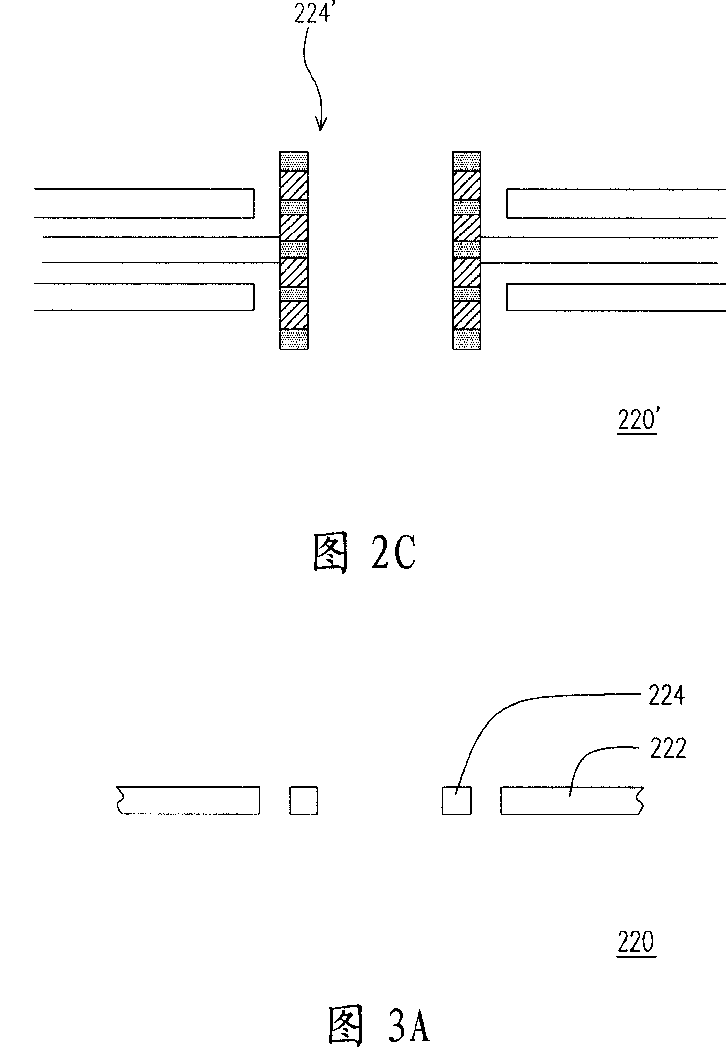
[0053] 2A is a schematic side sectional view of a chip package structure according to the first embodiment of the present invention, and FIG. 2B is a schematic top view of a lead frame of the chip package structure in FIG. 2A . Please refer to FIG. 2A and FIG. 2B , the chip package structure 200 of the first embodiment includes a chip 210 , a lead frame 220 , a plurality of first bonding wires 230 and a plurality of second bonding wires 240 . The chip 210 has an active surface 212 and a plurality of chip pads 214 , wherein the chip pads 214 are disposed on the active surface 212 . In addition, these chip pads 214 can be ground pads, power pads or signal pads.
[0054] The lead frame 220 is fixed on the chip 210 , and the lead frame 220 includes a plurality of inner leads 222 , at least one bus frame 224 , an insulating layer 226 and a plurality of transfer pads 228 . The bus frame 224 is located between the chip pads 214 and the inner pins 222 , and the insulation layer 226 i...
no. 2 example
[0064] 4A is a schematic side sectional view of a chip package structure according to a second embodiment of the present invention, and FIG. 4B is a schematic top view of a lead frame of the chip package structure in FIG. 4A . Please refer to FIG. 4A and FIG. 4B, the main difference between the chip package structure 300 of the second embodiment and the chip package structure 200 of the first embodiment is that: the lead frame 320 of the chip package structure 300 includes a chip seat P, a plurality of The inner pin 322 , at least one busbar 324 , an insulating layer 326 and a plurality of transfer pads 328 . The wafer 310 is disposed on the wafer seat P, and the active surface 312 is away from the wafer seat P. As shown in FIG. In other words, with respect to the relative position of FIG. 4A , the active surface 312 of the chip 310 is facing upward. In addition, the busbar 324 is located between the wafer pad P and the inner pins 322 .
[0065] The manufacturing method of t...
PUM
 Abstract
Description
Claims
Application Information
 - R&D
- Intellectual Property
- Life Sciences
- Materials
- Tech Scout
- Unparalleled Data Quality
- Higher Quality Content
- 60% Fewer Hallucinations
Browse by: Latest US Patents, China's latest patents, Technical Efficacy Thesaurus, Application Domain, Technology Topic, Popular Technical Reports.
© 2025 PatSnap. All rights reserved.Legal|Privacy policy|Modern Slavery Act Transparency Statement|Sitemap|About US| Contact US: help@patsnap.com


