
Patsnap Eureka
For R&D, Patsnap Eureka makes reading and utilizing patents & technical documents easy.
Patsnap Eureka AIR
Designed for self-driven R&D workflows. Generate viable solutions, solve complex R&D challenges, empower your innovation with AI.

Patsnap Eureka Materials
Designed for material experts only. Revolutionize your material R&D, from search, analyze, to developing new materials.

TechResearch
Generate reliable direction feasibility study reports for your R&D in just a few steps.

TechSeek
Discover and master advanced knowledge NOW. Basics, ideas, possibilities, all at once.

TechMind
As an expert in R&D Theories, TechMind can generates customized viable solutions instantly.

TechRisk
Analyze your overall solution with one click, know your potential R&D risks in advance.

TechMonitor
Get weekly tech updates, stay abreast of the latest tech innovations and key insights.
Ink jet printing head and its producing method
A printing head and inkjet technology, applied in the field of inkjet printing head and its manufacturing, can solve the problems of poor adhesion between the chamber layer and the wafer, and achieve the effect of improving the poor adhesion and improving the compatibility.
- Summary
- Abstract
- Description
- Claims
- Application Information
AI Technical Summary
Problems solved by technology
Method used
Image

Examples
no. 1 example
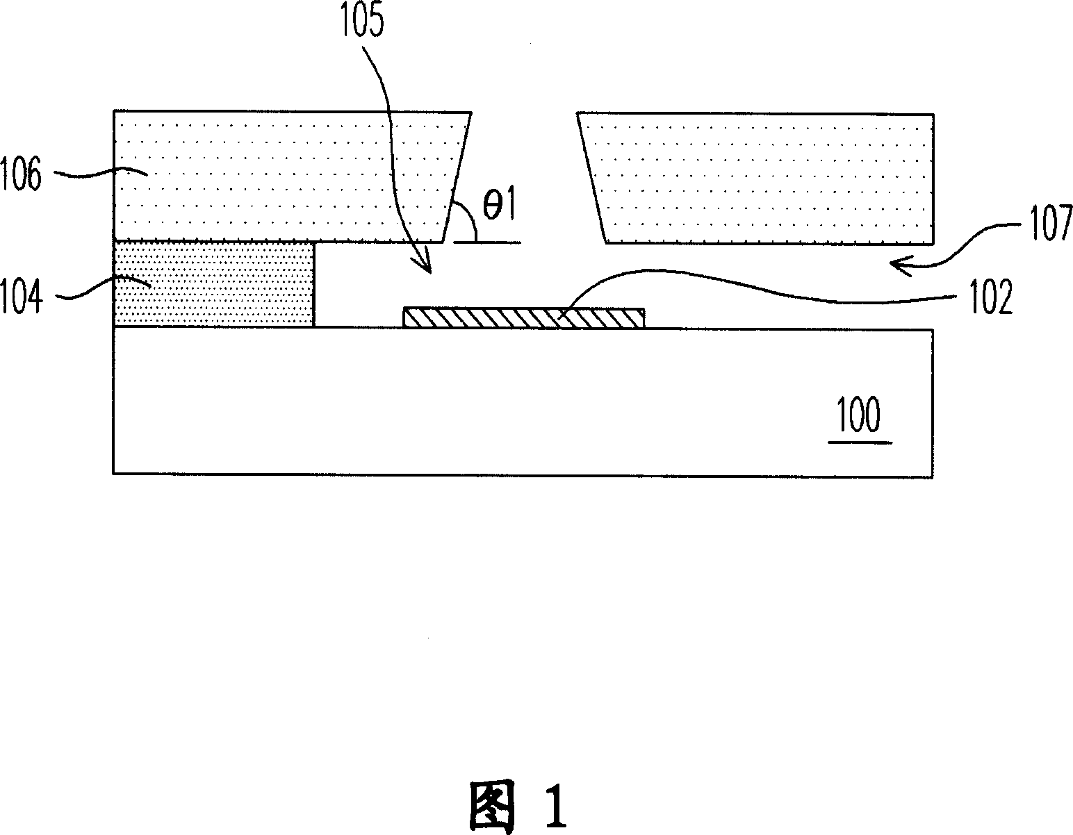
[0051] FIG. 1 is a schematic cross-sectional view of an inkjet printhead according to a first embodiment of the present invention.
[0052] Please refer to FIG. 1 , the inkjet print head of the first embodiment includes a chip (chip) 100, a chamber layer 104 and a nozzle layer 106, wherein the chip 100 has an actuating device 102, and the chamber layer 104 is disposed on the chip 100 , while the nozzle layer or nozzle plate 106 is disposed on the chamber layer 104 . Wherein, the chamber layer 104 generally has a plurality of chambers 105 , and the chambers are located above the actuating device 102 . In a preferred embodiment, the chamber layer 104 has a plurality of channels 107 respectively connected to the chambers. In a preferred embodiment, if the actuating device 102 is a heating element (heater; resistive element; or electric heating element), it will be covered with other protective layer (not shown), such as SiN layer, SiC layer or stack of SiN and SiC. Therefore, ...
no. 2 example
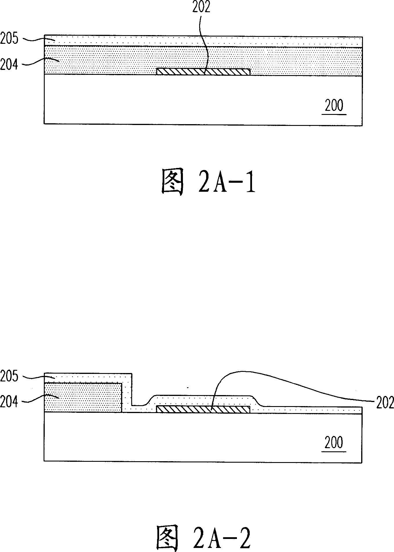
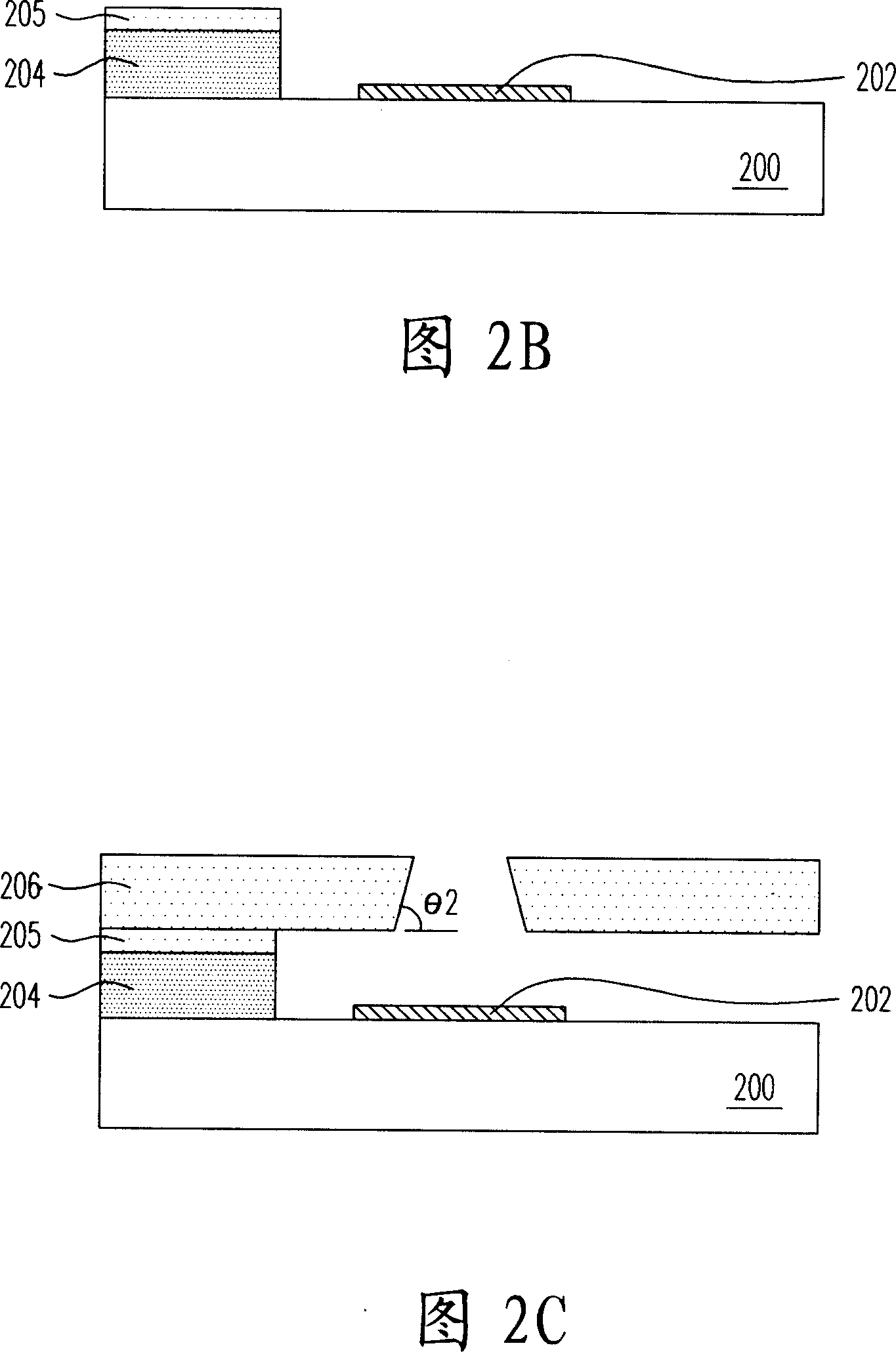
[0055] 2A-1, FIG. 2A-2 to FIG. 2C are schematic cross-sectional views of the manufacturing process of an inkjet printhead according to the second embodiment of the present invention, and the inkjet printhead produced in the second embodiment is the same as that in the first embodiment The difference of the example is that there is an additional first material layer between the chamber layer and the nozzle layer.
[0056] Please refer to FIG. 2A-1 and FIG. 2B first, a wafer 200 having a plurality of actuating devices 202 is provided, and the actuating devices 202 can be electric heating elements or piezoelectric elements. Afterwards, a double-layer structure is formed on the wafer 200 , which includes a chamber layer 204 in contact with the surface of the wafer 200 and a first material layer 205 not in contact with the surface of the wafer 200 . Therefore, the method shown in FIG. 2A-1 can be chosen to firstly form an organic solvent-developable acrylic negative photoresist (ie...
no. 3 example
[0060] 3A to 3B are schematic cross-sectional views of the manufacturing process of an inkjet printhead according to the third embodiment of the present invention, and the difference between the inkjet printhead manufactured in the third embodiment and the first embodiment is that it is located in the chamber There is also a second material layer between the layer and the nozzle layer.
[0061] Referring first to FIG. 3A , a wafer 300 having a plurality of actuating devices 302 is provided, and the actuating devices 302 may be electric heating elements or piezoelectric elements. Afterwards, a chamber layer 304 is formed on the wafer 300 . This chamber layer 304 has a plurality of chambers 305 and a plurality of flow channels 307 respectively connected to the chambers 305, and the chambers are located above the actuating device 302, and the material of the chamber layer 304 is organic solvent-developable acrylic It is a negative photoresist, and the preferred material is an or...
PUM
 Abstract
Description
Claims
Application Information
 - R&D Engineer
- R&D Manager
- IP Professional
- Industry Leading Data Capabilities
- Powerful AI technology
- Patent DNA Extraction
Browse by: Latest US Patents, China's latest patents, Technical Efficacy Thesaurus, Application Domain, Technology Topic, Popular Technical Reports.
© 2024 PatSnap. All rights reserved.Legal|Privacy policy|Modern Slavery Act Transparency Statement|Sitemap|About US| Contact US: help@patsnap.com