Material for use in the manufacturing of luminous display devices
A device, oxide technology, applied in organic light-emitting diodes, materials used in organic light-emitting diodes, preparing the field of materials, can solve the problems of chemical stability and low conductivity, etc.
- Summary
- Abstract
- Description
- Claims
- Application Information
AI Technical Summary
Problems solved by technology
Method used
Image
Examples
Embodiment 1
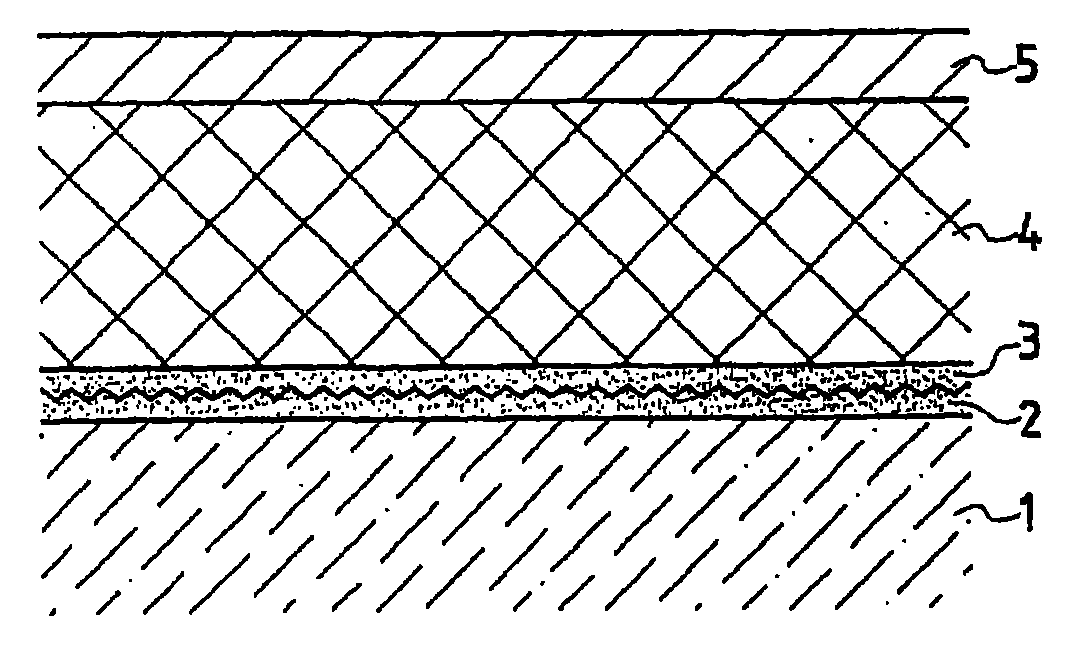
[0140] Example 1: Glass support coated with ITO layer and ATO layer
[0141] 1. A product sold by Samsung Corning Co., which uses a vacuum spraying technique to coat an ITO layer on a glass substrate of 0.7 mm was used.
[0142] This ITO layer has the following properties:
[0143] · Thickness is 192nm,
[0144] · The surface impedance is 7.6Ω / □,
[0145] · Average roughness (Rrms) measurement 5μm 2 4.7nm,
[0146] · Peak-valley roughness (Rpv) measurement 5μm 2 31.1nm,
[0147] · Working performance between 4.3-4.6eV,
[0148] · Transmittance is 83% within the visible range.
[0149] 2. The coating solution is prepared by adding tin dichlorodiacetate SnCl 2 (OAc) 2 Dissolve in ethanol with the addition of 4-hydroxy-4-methyl-pentanone (CAS 123-42-2) as a stabilizer. The relative amounts of tin and antimony were calculated to be 7 mol% for the final doping. The concentration of the stabilizer relative to tin was 2 mol%. Ethanol was added to give a final tin concentr...
Embodiment 2
[0159] Embodiment 2 (comparison)
[0160] For comparison purposes, a layer of ATO was directly deposited on a glass substrate with the same precursor solution used in Example 1 under the same deposition and heat treatment conditions, but no coated ITO layer was present on the glass substrate.
[0161] The properties of the resulting coating are:
[0162] · Surface impedance: 1890Ω / □,
[0163] · Optical transmittance: 85%,
[0164] · Working performance: 4.8 to 5.2eV,
[0165] Coating thickness: 108nm,
[0166] · Average roughness (Rrms): at 100nm 2 Measured within a square area to be 1nm,
[0167] · Peak-valley roughness (Rpv): at 100nm 2 Measured within the square area to be 3.6nm,
Embodiment 3
[0168] Embodiment 3 (comparison)
[0169] For comparison purposes, eight consecutive ATO layers were deposited directly on the substrate with the same precursor solution as used in Example 2 under the same deposition and thermal post-treatment conditions.
[0170] The properties of these coatings are:
[0171] · Surface impedance: 50 to 55Ω / □,
[0172] · Optical transmittance: 65%,
[0173]· Working performance: 4.8 to 5.2eV,
[0174] Coating thickness: 600nm,
[0175] · Average roughness (Rrms) measurement 100nm 2 The square area is 2.5nm,
[0176] · Peak-valley roughness (Rpv) measurement 100nm 2 The square area is 8nm,
[0177] The properties of supports coated only with an ITO layer, the coated supports according to inventive example 1 (ATO / ITO) and the coated supports according to comparative examples 2 and 3 are listed in the table below:
[0178] ITO
PUM
| Property | Measurement | Unit |
|---|---|---|
| surface roughness | aaaaa | aaaaa |
| surface roughness | aaaaa | aaaaa |
| thickness | aaaaa | aaaaa |
Abstract
Description
Claims
Application Information
 - R&D
- Intellectual Property
- Life Sciences
- Materials
- Tech Scout
- Unparalleled Data Quality
- Higher Quality Content
- 60% Fewer Hallucinations
Browse by: Latest US Patents, China's latest patents, Technical Efficacy Thesaurus, Application Domain, Technology Topic, Popular Technical Reports.
© 2025 PatSnap. All rights reserved.Legal|Privacy policy|Modern Slavery Act Transparency Statement|Sitemap|About US| Contact US: help@patsnap.com


