Exposure method, exposure apparatus, and device manufacturing method
A technology of exposure device and exposure method, applied in the field of device manufacturing, capable of solving problems such as damage, unevenness of optical characteristics, defects, etc.
- Summary
- Abstract
- Description
- Claims
- Application Information
AI Technical Summary
Problems solved by technology
Method used
Image
Examples
Embodiment Construction
[0025] Next, an embodiment of the present invention will be described based on FIGS. 1 to 6 .
[0026] FIG. 1 schematically shows the configuration of an exposure apparatus 100 according to an embodiment. The exposure apparatus 100 is a scanning exposure apparatus of a step-and-scan method, that is, a so-called scanner.
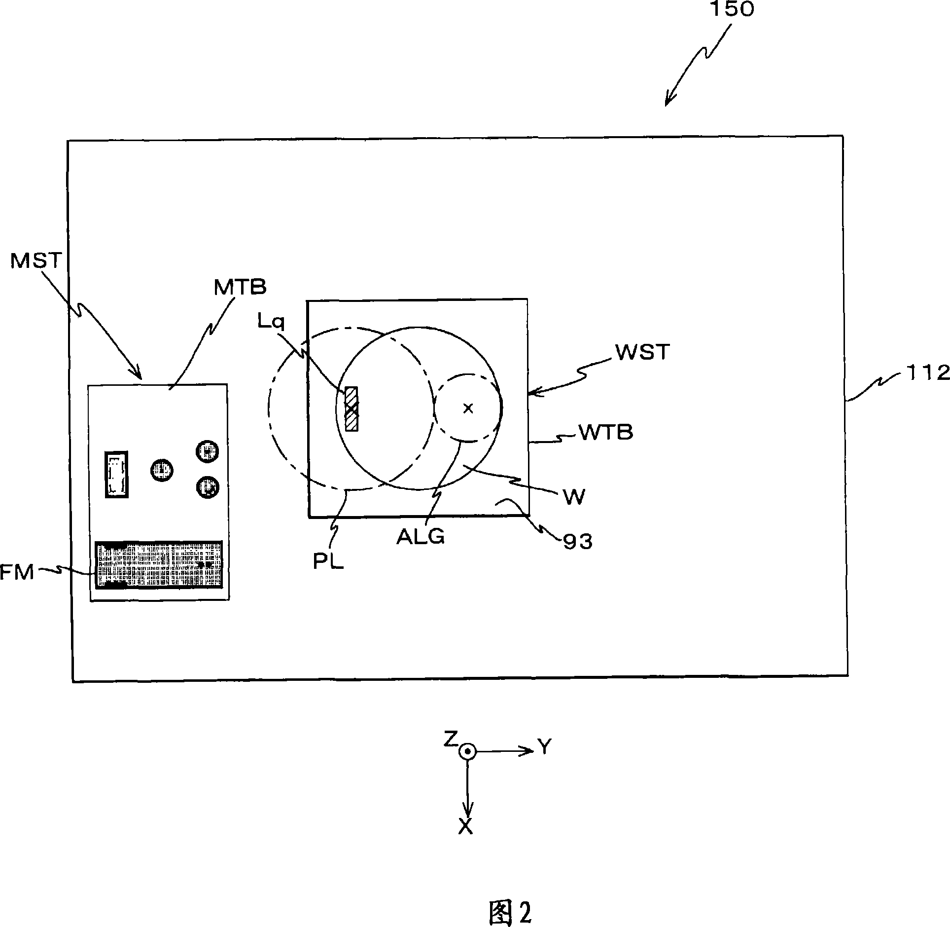
[0027] The exposure apparatus 100 includes: an illumination system ILS; and a master stage RST that holds a master R and moves in a predetermined scanning direction (here, the left-right direction in FIG. 1 , that is, the Y-axis direction). The master is a mask illuminated by the exposure light IL as an energy beam from the illumination system ILS; the projection unit PU includes projection optics for projecting the exposure illumination light IL emitted from the master R onto the wafer W; System PL; stage device 150 including wafer stage WST as an object stage on which wafer W is placed; measurement stage MST used for measurement for exposure; and their con...
PUM
 Abstract
Description
Claims
Application Information
 - R&D
- Intellectual Property
- Life Sciences
- Materials
- Tech Scout
- Unparalleled Data Quality
- Higher Quality Content
- 60% Fewer Hallucinations
Browse by: Latest US Patents, China's latest patents, Technical Efficacy Thesaurus, Application Domain, Technology Topic, Popular Technical Reports.
© 2025 PatSnap. All rights reserved.Legal|Privacy policy|Modern Slavery Act Transparency Statement|Sitemap|About US| Contact US: help@patsnap.com


