Method for forming light absorbing layer in cis-based thin film solar battery
A technology for solar cells and light-absorbing layers, applied in coatings, circuits, photovoltaic power generation, etc., can solve the problems of increased production costs, expensive, complex structures, etc., and achieve the effect of improving performance and product yield
- Summary
- Abstract
- Description
- Claims
- Application Information
AI Technical Summary
Problems solved by technology
Method used
Image
Examples
Embodiment Construction
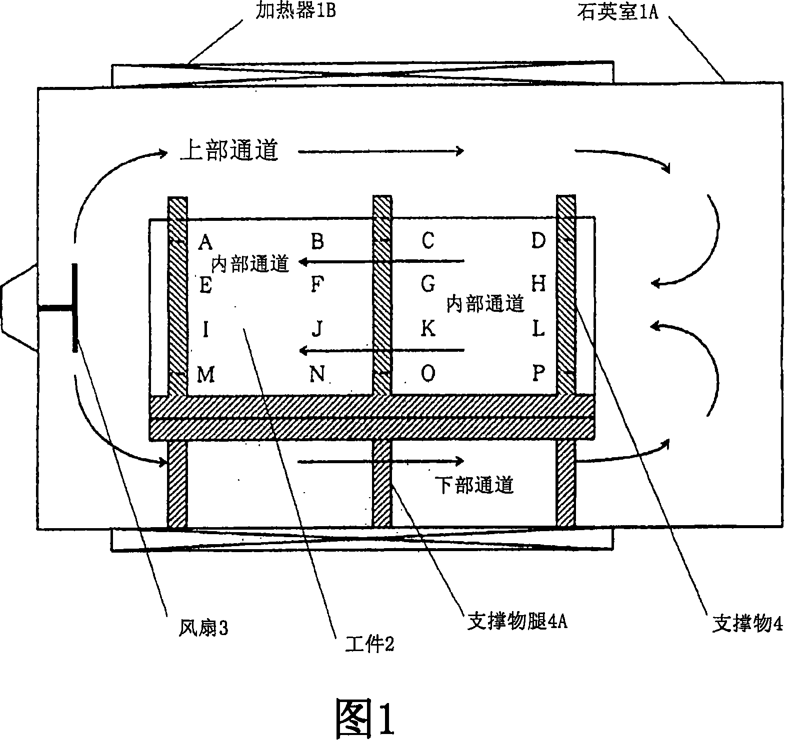
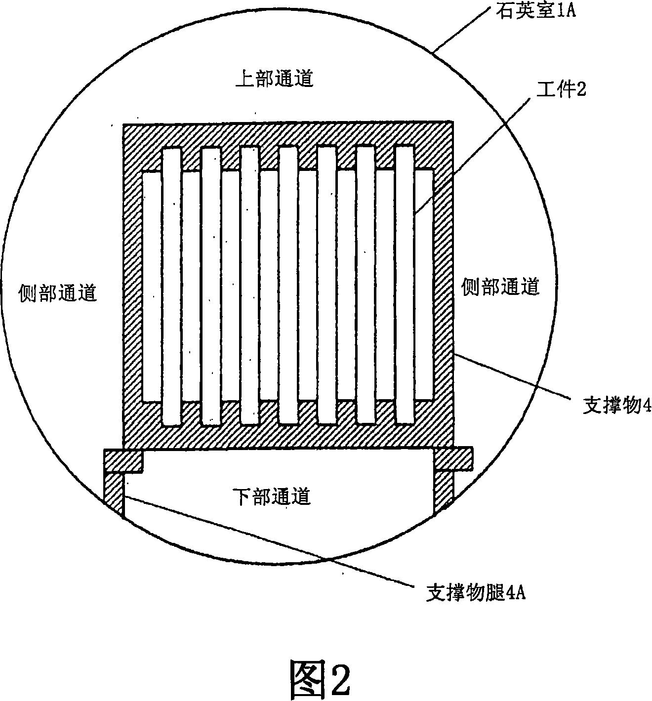
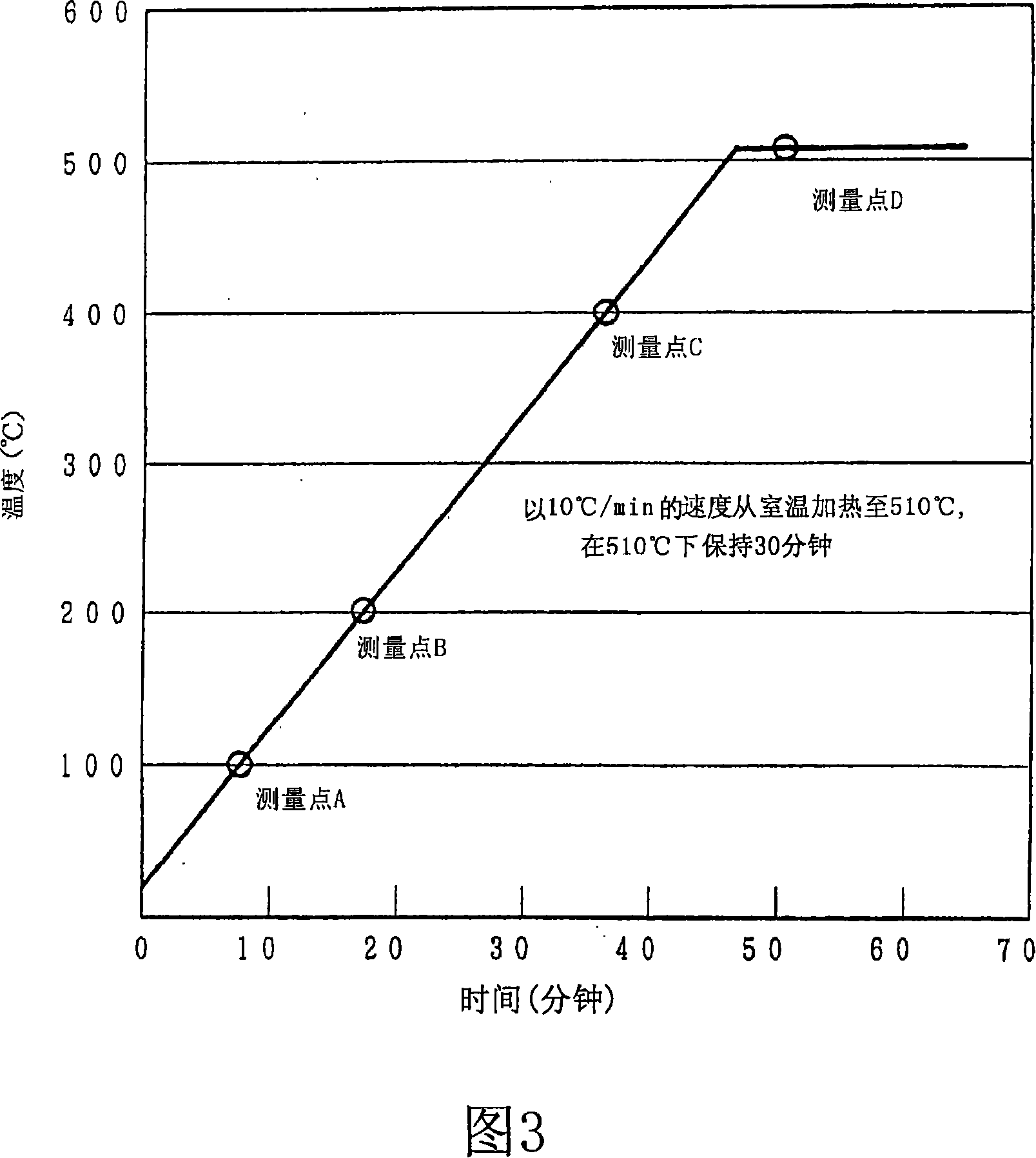
[0052] The present invention provides a method of film formation for use in the step of forming a film by selenization, sulfurization / selenization, sulfurization, or selenization / sulfurization in the step of forming a CIS light absorbing layer in a CIS type thin film solar cell . As shown in Figure 7, the CIS type thin film solar cell 5 is a pn heterojunction device, which has a glass substrate 5A, a metal backing electrode layer 5B, a p-type CIS light absorbing layer 5C, a high resistance The substrate structure of the buffer layer 5D and the n-type window layer (transparent conductive film) 5E. When forming the CIS light absorbing layer 5C, Cu / Ga (workpiece 2A), Cu / In (workpiece 2B) and Cu-Ga shown in FIG. 5 will be included on the metal back electrode layer on the glass substrate. The metal precursor film of the multilayer structure of any one of In / In (workpiece 2C) (hereinafter referred to as the workpiece to be processed for film formation) is subjected to a film format...
PUM
 Abstract
Description
Claims
Application Information
 - R&D
- Intellectual Property
- Life Sciences
- Materials
- Tech Scout
- Unparalleled Data Quality
- Higher Quality Content
- 60% Fewer Hallucinations
Browse by: Latest US Patents, China's latest patents, Technical Efficacy Thesaurus, Application Domain, Technology Topic, Popular Technical Reports.
© 2025 PatSnap. All rights reserved.Legal|Privacy policy|Modern Slavery Act Transparency Statement|Sitemap|About US| Contact US: help@patsnap.com


